Daejeon's Semiconductor Sector Produces World-Class Research and Loses the Engineers Who Commercialise It
Daejeon is home to the highest density of semiconductor-related public R&D investment per capita in South Korea. At KRW 2.1 million per resident, it exceeds Suwon by more than double. It houses KRICT, KAERI, KAIST, and ETRI within a single metropolitan area. It generated 94 technology transfer cases from public research institutes to private companies in 2024 alone, with 61% flowing directly into materials and equipment manufacturing. By every input measure, Daejeon should be the country's dominant centre for semiconductor equipment commercialisation.
It is not. The city trains and incubates advanced materials talent at scale, then watches that talent leave. KAIST-trained engineers who enter Daejeon firms command an 8 to 12% starting salary premium over Seoul National University peers. Within five years, 58% of them have relocated to Gyeonggi province. KNC Corporation, a specialist in optical components, lost a quarter of its senior optical designers in a single quarter of 2024 and responded not by raising Daejeon salaries but by opening an office in Pangyo. Only 23% of technologies transferred from research institutes to private firms reach commercial production scale within three years. The city's R&D engine runs hot. Its commercialisation pipeline leaks.
What follows is an analysis of the forces pulling Daejeon's semiconductor equipment sector in two directions at once: a research base that generates demand for specialised talent and an industrial structure that cannot hold it. For hiring leaders competing in this market, the implications are specific, the constraints are physical, and the search methods required to fill critical roles here differ from what works in Seoul or Suwon.
Daejeon's Semiconductor Equipment Cluster in 2026: Scale, Revenue, and the Shape of the Market
Daejeon's advanced materials and semiconductor equipment manufacturing sector now encompasses roughly 340 enterprises employing an estimated 12,800 workers directly, as recorded at the close of 2024. That headcount represents 18% growth from 2022, outpacing the 14% national semiconductor employment growth rate tracked by the Korea Semiconductor Industry Association. The sector generated consolidated revenues of approximately KRW 4.2 trillion (USD 3.1 billion) in 2024. SME revenue growth averaged 12% year-over-year, compared to 8% for large enterprises, a pattern consistent with successful commercialisation of research institute spin-offs gaining traction.
The Daejeon metropolitan government's 2026 target of 14,700 direct sector jobs assumes completion of the Second Daedeok Valley Complex by mid-2026, which would add 45,000 square metres of R&D and light manufacturing space. KRW 890 billion in private investment has been announced for 2025 to 2026, distributed primarily across specialty gases (KRW 320 billion), optical components (KRW 210 billion), and advanced ceramics (KRW 180 billion).
Here is the number that reframes every other figure in this article: 70% of that announced investment targets R&D centres or headquarters functions. Only 30% includes production facilities. Capital is flowing into Daejeon to develop technologies. It is not flowing in to manufacture them at scale. This distinction governs the talent dynamics of the entire market. Daejeon's employers are not hiring production engineers for volume manufacturing lines. They are hiring research-adjacent specialists who can bridge the gap between laboratory and pilot production. That role category barely exists as a defined career path, which is precisely why it is so difficult to fill.
The Research Infrastructure That Creates Demand and the Physical Constraints That Limit Supply
Daedeok Innopolis and the Institutes That Anchor the Ecosystem
The Daedeok Research and Development Special Zone spans 27.8 square kilometres and houses 28 research institutes alongside 1,380 tenant companies. For executive hiring in advanced materials and industrial manufacturing, the four anchor institutions define the market.
KRICT operates with 1,400 researchers and a 2024 budget of KRW 312 billion. Its Semiconductor Chemicals Commercialisation Centre supports 34 active spin-offs. KRICT reported 187 active technology transfer contracts with regional firms, generating KRW 32.4 billion in licensing revenue. KAIST, with 10,500 students and faculty, holds 412 active patents in semiconductor manufacturing equipment and supplies both talent and intellectual property to the cluster. ETRI contributes equipment automation and sensor development. KAERI's direct commercialisation impact on semiconductor equipment is secondary but meaningful in radiation processing and advanced materials.
The Daejeon Techno Valley in Yuseong-gu houses an additional 156 advanced materials SMEs with shared pilot production facilities. The National NanoFab Centre provides 2,400 square metres of Class 100 to 1000 shared cleanroom space for prototyping.
The Cleanroom Bottleneck
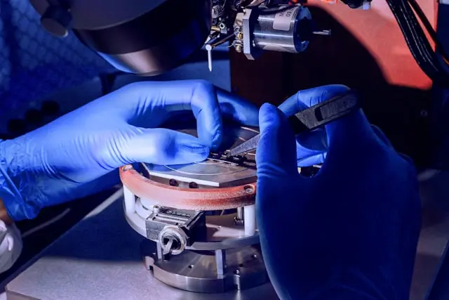
The physical constraint is not abstract. Vacancy rates for Class 1000 or better cleanroom space in Daejeon stand at 4.2%, which means effectively full. Waiting lists for SME-scale facilities of 500 to 2,000 square metres extend 8 to 14 months, according to CBRE Korea's Q4 2024 industrial market report. KRICT's own 8,500 square metre pilot plant for specialty chemical scale-up operates at 94% capacity.
A company that has developed a novel CMP slurry additive or specialty gas formulation in Daejeon and wants to scale production faces a physical queue. The average capital required to build a Class 1000 production line for specialty chemicals runs KRW 8 to 12 billion (USD 6 to 9 million), beyond typical SME debt capacity. Government matching funds under the K-Semiconductor Belt initiative require 1:1 equity participation that most founders cannot meet. As of December 2024, only 34% of the KRW 120 billion in allocated matching funds had been committed. The bottleneck is not ideas. It is not even money, strictly speaking. It is the physical infrastructure required to turn a licensed technology into a product that ships.
This is what forces dual-facility operations. Companies like Wonik and TES maintain R&D in Daejeon and production in Cheonan or Dangjin. Zoning restrictions within the research zone prevent heavy manufacturing, including forging and large-scale casting. The result is a split workforce where the most senior engineers commute or relocate, creating the retention fragility that defines this market.
Why Daejeon's Talent Shortage Is Not a Shortage of People
Job postings for semiconductor equipment and materials roles in Daejeon increased 34% year-over-year in 2024, against 22% nationally. Average time-to-fill for technical positions extended to 68 days, up from 45 days in 2022. These headline figures suggest a conventional supply-demand imbalance. The reality is more specific and more difficult.
Daejeon does not lack engineers. KAIST and the research institutes produce a steady flow of materials scientists, chemical engineers, and optical specialists. Entry-level materials scientists and general mechanical engineers show active job-seeking behaviour at a 2:1 active-to-passive ratio. The market for junior talent is functional, if imperfect.
The scarcity concentrates in three role categories where the required experience cannot be trained in a university or formed in a laboratory. It can only be accumulated inside an operating semiconductor fabrication or equipment manufacturing facility. This is a shortage of engineers whose skills were built through years of production-floor problem-solving. KAIST does not produce them. KRICT does not produce them. Samsung's fabs and SK Hynix's cleanrooms produce them. And those facilities are in Hwaseong, Pyeongtaek, Icheon, and Cheongju. Not Daejeon.
Vacuum Technology and Precision Mechanics Engineers
The shift to atomic layer deposition and high-vacuum etch equipment has intensified demand for engineers who understand ultra-high vacuum system design, leak detection, and outgassing control. Daejeon has 340 registered engineers with vacuum technology certifications, according to the Korea Vacuum Society member directory. Estimated demand exceeds 520.
A mid-sized optical coating equipment manufacturer in the Daejeon Techno Valley cluster kept a Senior Vacuum System Engineer position open for 11 months throughout 2024. It eventually filled the role with a candidate relocated from Busan at a 35% premium above standard salary bands. The Daejeon Chamber of Commerce documented six similar cases in its 2024 SME Hiring Survey. Senior vacuum technology engineers in this market have an unemployment rate below 1.2%, average tenure of 6.8 years, and an active-to-passive candidate ratio below 1:4. They do not post resumes on job boards. Reaching them requires direct identification of passive candidates through industry society networks and targeted outreach.
Chemical Process Engineers with Fab-Scale Experience
The gap between laboratory synthesis and ISO-Class 5 manufacturing is where Daejeon's commercialisation pipeline most frequently breaks. Local universities produce approximately 180 relevant graduates annually. Industry requires more than 340. The shortfall in raw numbers is only half the problem. What the market truly lacks is engineers who have operated at fab scale, managing contamination control at parts-per-trillion levels in a production environment rather than a research setting.
KRICT spin-off companies in CMP slurry and photoresist development have resorted to systematic poaching from each other. Signing bonuses for senior engineers with seven or more years of experience have reached KRW 50 million (USD 37,000), an unusual practice for SMEs of this scale, according to the Korea Venture Capital Association's October 2024 report on Daejeon deep tech hiring practices. Chemical process engineers with Samsung or SK Hynix fab backgrounds receive three to five unsolicited offers monthly during market peaks. Job board activity from this population indicates distress or imminent departure, not availability.
Optical System Design Engineers
Daejeon has inherent strength here. KAIST's optical engineering programme is one of Asia's strongest. Yet retention is the problem, not production. According to Electronic Times Korea, KNC Corporation lost 3 of 12 senior optical designers in Q3 2024 to competitors in Suwon and Shanghai. The company's response was to establish a satellite R&D office in Pangyo to retain talent unwilling to commute to Daejeon. This pattern, where a Daejeon employer opens a facility elsewhere to keep the people it has already hired, is a direct symptom of the ecosystem thinness described in the research.
Optical system architects occupy a "hidden job market" where positions fill before public posting, through academic advisor networks at KAIST and POSTECH and through conference recruitment at Korean Optical Society events. The passive candidate ratio is estimated at 78%.
The Original Tension: R&D Density Does Not Automatically Create an Industrial Cluster
The analytical claim that runs through this market is counter-intuitive and worth stating directly. Daejeon disproves the common policy assumption that concentrating public R&D investment in a single geography will generate a self-sustaining industrial cluster. The city has the research. It has the institutes. It has the patents. What it does not have is the production infrastructure, the employer density, or the career trajectory depth that causes senior engineers to stay past the five-year mark.
This is not a funding problem, and it is not a talent production problem. It is a conversion problem. Daejeon invests KRW 2.1 million in semiconductor R&D per resident. Suwon invests KRW 890,000. Yet Suwon retains 61% of its technical workforce over five years while Daejeon retains 42%. The difference is that Suwon offers something Daejeon cannot: a dense ecosystem where an engineer who wants to change employers, pivot their specialisation, or advance into a leadership role can do so without moving house. In Daejeon, switching employers often means switching cities.
This matters for hiring leaders because it reframes the search challenge. A failed executive search in Daejeon is rarely a failure of offer quality. It is a failure to address the career trajectory calculation that every senior candidate makes. Compensation at Daejeon firms already adjusts for cost of living. The 15 to 20% discount to Suwon or Pangyo is offset by a 25 to 30% lower cost of living. The real friction is that a candidate's spouse has fewer career options. The next job after this one is less visible. The professional network is thinner. These are not problems that a signing bonus resolves.
Compensation Benchmarks and the Geographic Premium Calculus
CTO and VP Engineering Roles
At the CTO or Senior VP level, with 15 or more years of experience, C-level executive compensation in Daejeon's semiconductor equipment sector ranges from KRW 350 to 500 million annually (USD 260,000 to 370,000), with stock options available at listed entities. Director-level roles at 10 to 15 years command KRW 220 to 300 million (USD 165,000 to 225,000).
The Suwon and Hwaseong premium for equivalent roles runs 20 to 25% above Daejeon. Pangyo adds 15 to 20% with a stronger equity compensation culture. Hsinchu in Taiwan pushes the gap to 30 to 40% for senior roles, with additional tax incentives for foreign experts and exposure to leading-edge 3nm and 2nm process development that Korea's current licensing structure does not offer domestically.
General Manager and Plant Manager Roles
General managers overseeing pilot-to-commercial production transitions at unlisted SMEs earn KRW 120 to 180 million (USD 90,000 to 135,000). Plant managers at larger enterprises command KRW 180 to 250 million (USD 135,000 to 185,000). The Korea SMEs and Startups Agency identified a severe shortage of executives combining semiconductor industry experience with SME financial management capabilities. This hybrid profile, someone who understands both a cleanroom process flow and an SME balance sheet, is exceptionally rare.
Commercialisation and Business Development Leaders
Heads of business development at research institute spin-offs, responsible for technology licensing negotiation, chaebol partnerships, and Series B or C fundraising, earn base salaries of KRW 100 to 160 million with meaningful equity components. The variability is high. Negotiating compensation in this tier depends heavily on the spin-off's stage, IP portfolio strength, and proximity to a specific customer commitment.
The net effect of Daejeon's compensation structure is that it is rational on paper and insufficient in practice. The cost-of-living adjustment closes much of the nominal gap with Seoul and Gyeonggi. But the candidates who would fill these roles are not making a spreadsheet calculation. They are making a career calculation. And that calculation increasingly favours markets with denser employer ecosystems.
The Regulatory and Geopolitical Environment Reshaping This Market
K-REACH and the Cost of Compliance
K-REACH compliance costs for new semiconductor materials average KRW 450 million per substance. This figure alone explains why large chemical conglomerates can introduce new materials into the Korean market while Daejeon SMEs struggle. A spin-off with KRW 2 billion in annual revenue cannot absorb a KRW 450 million registration cost for a single new product. The regulatory burden is not merely administrative. It is a competitive barrier that favours scale and penalises the exact kind of innovation-stage company that Daedeok Innopolis exists to support.
Export Controls and the China Revenue Risk
U.S. CHIPS Act alignment requirements and Japanese export control coordination have created material compliance burdens for Daejeon companies supplying Chinese fabs. According to the Korea International Trade Association's 2024 regional export survey, 23% of local equipment and materials SMEs reported order cancellations or delays due to export licensing. Daejeon's specialty sensor and component suppliers historically derived 35 to 45% of revenue from China-bound shipments. China's accelerated domestication of semiconductor equipment components now threatens that revenue base directly.
This is not a future risk. It is a present condition. Companies that built their commercial models around Chinese demand are recalculating. The talent implication is that business development leaders in this market need export compliance expertise alongside commercial skills. AI-enabled talent mapping can identify professionals who combine both, but the pool is small and concentrated in Seoul.
The PhD Pipeline Problem
KAIST and local universities have seen a 12% decline in domestic PhD enrolment in materials science between 2020 and 2024. Students are pivoting to AI and software. The immediate hiring impact is manageable; the five-to-ten-year impact on Daejeon's research commercialisation pipeline is serious. Fewer domestic PhDs means fewer founders of the next generation of KRICT spin-offs. It also means the hiring leaders of 2030 will face an even thinner candidate pool for the roles that are already hardest to fill today.
What This Market Requires from a Search Strategy
Traditional recruitment methods reach a fraction of the viable candidate pool in Daejeon's semiconductor equipment sector. The three most critical role categories, vacuum technology engineers, chemical process engineers with fab experience, and optical system architects, are overwhelmingly passive. Active-to-passive ratios run below 1:4 for senior vacuum engineers and as low as 22% active for optical designers. A job posting on Saramin or LinkedIn reaches, at best, the candidates who are already thinking about leaving. In a market where 80% of the best candidates are not actively looking, that approach structurally underperforms.
The search method that works in this market has three characteristics. First, it begins with systematic talent mapping of the 340-odd enterprises in the cluster, the research institute alumni networks, and the Korea Vacuum Society and Korean Optical Society membership directories. Second, it accounts for the geographic premium calculation by presenting a complete proposition that addresses career trajectory, not just compensation. Third, it moves fast. A 68-day average time-to-fill means the strongest candidates disappear mid-process. A search that delivers interview-ready candidates in 7 to 10 days operates in a different competitive bracket from one that takes three months to assemble a shortlist.
KiTalent's approach to executive search in advanced manufacturing is built around exactly this model. AI-powered candidate identification reaches passive professionals who are invisible to job boards. Pay-per-interview pricing means clients invest only when they are meeting qualified candidates, not funding months of speculative sourcing. With a 96% one-year retention rate across 1,450 executive placements, the model addresses the retention concern that haunts every Daejeon hire.
For organisations hiring CTO, VP Engineering, or Plant Manager roles in Daejeon's semiconductor equipment and advanced materials sector, where the candidates you need are solving problems inside competitor facilities and will not respond to a job advertisement, speak with our executive search team about how we identify and engage the talent this market cannot surface through conventional methods.
Frequently Asked Questions
Why is it so difficult to hire semiconductor equipment engineers in Daejeon?
Daejeon's difficulty is specific. The city produces strong research talent through KAIST and KRICT but lacks the large-scale fabrication facilities where engineers accumulate production-floor experience. Vacuum technology engineers, chemical process engineers with fab backgrounds, and optical system architects are overwhelmingly passive candidates with unemployment rates below 1.2%. Job postings in Daejeon increased 34% in 2024 while time-to-fill extended to 68 days. Reaching these candidates requires direct headhunting through industry networks rather than job board advertising, which reaches fewer than 25% of the viable pool in the most critical role categories.
What do senior semiconductor engineers earn in Daejeon compared to Suwon or Pangyo?
CTO and Senior VP roles in Daejeon pay KRW 350 to 500 million annually (USD 260,000 to 370,000). Suwon and Hwaseong offer a 20 to 25% premium for equivalent positions. Pangyo adds 15 to 20%. However, Daejeon's cost of living is 25 to 30% lower than these markets, which narrows the real gap. The compensation differential alone does not explain retention challenges; career trajectory options and ecosystem density are the primary drivers of attrition among mid-career and senior engineers.
What is Daedeok Innopolis and why does it matter for semiconductor hiring?
Daedeok Innopolis is a 27.8 square kilometre research and development special zone in Daejeon housing 28 research institutes and 1,380 tenant companies. It anchors Korea's highest concentration of semiconductor-related public R&D investment per capita. KRICT, KAIST, KAERI, and ETRI all operate within it. In 2024, 94 technology transfers flowed from institutes to private companies, with 61% targeting materials and equipment sectors. For hiring leaders, Daedeok represents both the talent source and the retention challenge: graduates enter local firms at premium salaries but leave the region within five years at a 58% rate.
How do export controls affect Daejeon's semiconductor equipment companies?
U.S. CHIPS Act and Japanese export control alignment requirements have created direct commercial disruption. In 2024, 23% of Daejeon equipment and materials SMEs reported order cancellations or delays due to export licensing issues. Companies that historically derived 35 to 45% of revenue from China-bound shipments face sustained revenue risk from China's push to domesticate semiconductor components. This means business development and compliance leadership roles now require export control expertise alongside commercial capabilities, further narrowing the candidate pool for executive roles across the semiconductor supply chain.
How can organisations improve retention of technical talent in Daejeon?
Compensation parity is necessary but not sufficient. Daejeon's 42% five-year retention rate versus 61% in Seoul and Gyeonggi reflects ecosystem thinness rather than pay gaps. Effective retention strategies address career trajectory visibility, spousal employment options, and internal mobility. Companies like KNC Corporation have opened satellite offices in Pangyo to retain engineers unwilling to remain in Daejeon full-time. For senior hires, structuring roles with hybrid or multi-site arrangements can widen the addressable talent pool materially while reducing the risk of early departure.
What role does KiTalent play in semiconductor executive recruitment in Korea?
KiTalent combines AI-powered talent mapping with direct headhunting to identify passive candidates in highly specialised markets. In a sector where fewer than 25% of senior engineers actively seek new roles, conventional job advertising consistently underperforms. KiTalent delivers interview-ready executive candidates within 7 to 10 days using a pay-per-interview model with no upfront retainer. With a 96% one-year retention rate and experience across 200 organisations globally, the approach is designed for markets where speed, precision, and access to non-visible talent determine whether a search succeeds or stalls.