Austin's Semiconductor Sector in 2026: The Hiring Gap That $25 Billion in Investment Has Not Closed
The Samsung Taylor fab is moving toward initial production shipments. AMD is expanding its Austin design campus by double digits. NXP has committed half a billion dollars to local facility upgrades. Yet the single greatest constraint on Austin's semiconductor future is not capital, not equipment, and not regulatory approvals. It is the absence of enough qualified human beings to operate what is being built.
Austin's semiconductor sector now accounts for roughly 8,000 to 9,000 direct manufacturing and R&D positions across its major facilities. That figure needs to grow by at least 800 to 1,200 additional process engineers, yield engineers, and equipment technicians in 2026 alone, just to support the Taylor ramp. The candidates who can fill those roles are overwhelmingly passive: 75 to 80 per cent of qualified professionals in critical semiconductor specialisms are employed, not looking, and not responding to job postings. In a market where technical roles already take 78 days to fill on average, compared to 52 for general technology positions, the maths do not favour the slow.
What follows is a ground-level analysis of where Austin's semiconductor talent shortages are most severe, what is driving them, why the conventional hiring playbook is failing, and what organisations competing for leadership talent in this market need to do differently before the window narrows further.
The Samsung Taylor Ramp Changes the Talent Equation
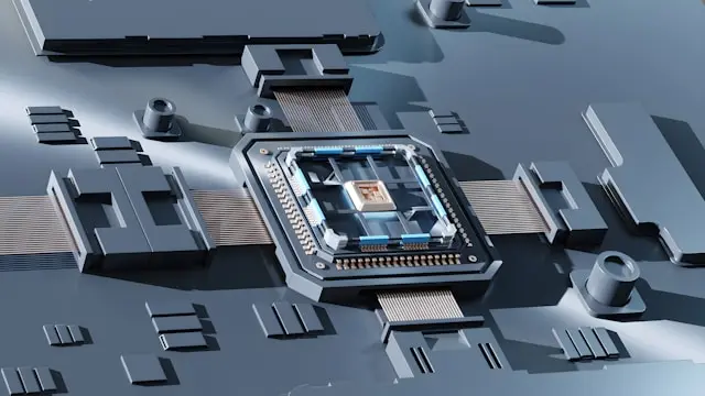
Samsung's $25 billion Taylor facility, located 17 miles northeast of Austin along SH-130, represents the single largest capital investment in Austin's semiconductor history. Cleanroom equipment installation commenced in Q3 2025. Industry analysis suggests the facility targets advanced logic nodes in the 4nm/5nm family, with initial production shipments expected by late 2026.
The workforce implications are immediate and concrete. Samsung has indicated a need for 2,000 to 3,000 personnel when Taylor reaches full operation. The 2026 recruitment requirement alone sits at 800 to 1,200 additional hires across process engineering, yield engineering, and equipment technician roles. These are not positions that can be filled through campus recruiting cycles or inbound applications. A process integration engineer at a leading-edge logic fab requires deep expertise in plasma etch, chemical vapour deposition, and atomic layer deposition at sub-7nm geometries. The number of people in the United States with that profile and no current employer is vanishingly small.
Samsung Austin Semiconductor already operates two established fabrication facilities employing approximately 3,000 to 3,500 people, producing 14nm and 28nm logic devices. The Taylor ramp does not replace those operations. It layers advanced-node demand on top of an existing workforce that is already under retention pressure. When a fab operator of this scale recruits 800-plus specialists in a single year from a market where the hidden 80 per cent of passive talent dominates every critical role category, the ripple effects extend well beyond Samsung's own hiring pipeline.
Every other semiconductor employer in the Austin corridor faces the same compressed labour pool, now under materially greater extraction pressure than at any point in the past decade.
AMD, NXP, and Applied Materials: The Compounding Demand Nobody Discusses
AMD's Design Campus Expansion
The Taylor ramp dominates headlines, but it is not the only source of hiring acceleration in Austin's advanced manufacturing and industrial sector. AMD maintains its largest U.S. design campus in Austin, employing approximately 2,500 to 3,000 staff focused on server CPU, GPU, and embedded processor architectures. The company has indicated 10 to 15 per cent headcount growth in Austin through 2026, concentrated in silicon design verification and systems architecture.
Design verification engineers fluent in SystemVerilog and UVM methodologies for complex system-on-chip validation are among the most sought-after professionals in the global semiconductor industry. AMD's Austin campus serves as the primary engineering hub for its EPYC server processor line. The roles being created are not entry-level. They require engineers who can validate architectures destined for hyperscale data centres, where a single design flaw discovered post-tapeout can cost hundreds of millions of dollars.
NXP and Applied Materials: Steady Pressure on a Thin Market
NXP Semiconductors operates a mixed-signal fab and design centre in Austin employing roughly 1,000 to 1,200 people, focused on automotive networking and secure identification. The company has committed $500 million to Austin facility expansion through 2027, though 2026 hiring growth is expected at a more modest 3 to 5 per cent. Applied Materials maintains approximately 1,500 to 2,000 employees in Austin across equipment engineering and process support functions.
Neither company generates the volume hiring pressure of Samsung or AMD individually. Collectively, however, they represent a persistent drain on the same finite talent pool. An equipment engineer leaving Applied Materials for Samsung Taylor, or an automotive mixed-signal designer moving from NXP to AMD, does not expand the regional talent supply. It merely redistributes scarcity. The net effect is that Austin's semiconductor employers are increasingly competing with each other rather than drawing net new talent into the market. This is the definition of a zero-sum hiring environment, and it is precisely the condition under which executive searches fail most frequently.
Where the Shortages Bite Hardest
Process Integration and Lithography Engineers
Process integration engineers at major Austin fabs typically see roles remain unfilled for 90 to 120 days, more than double the 45 to 60 day timeline that was standard as recently as 2019. Employers are frequently extending search timelines or lowering experience requirements to generate shortlists. Neither response solves the underlying problem. Extended timelines mean production targets slip. Lowered requirements mean less experienced engineers enter roles where mistakes destroy wafer lots worth millions.
Senior lithography engineers command signing bonuses of $50,000 to $75,000 above base compensation when moving between competitors. According to industry compensation reports referencing Radford Technology Survey data, Samsung and AMD cycle talent between Austin operations and Bay Area headquarters through retention equity packages equivalent to 18 to 24 months of salary. These are not standard retention tools. They are emergency measures deployed when an employer calculates that losing a single lithography specialist would cost more than paying them twice.
Yield Engineers and Advanced Packaging Specialists
The Taylor ramp introduces a specific category of demand that barely existed in Austin before: yield ramp optimisation for leading-edge logic. Yield engineering at advanced nodes requires a hybrid profile combining statistical process control with data science integration. These professionals must diagnose why a new process produces fewer working chips than projected and systematically close the gap. At a $25 billion fab, the financial distance between 60 per cent yield and 85 per cent yield is measured in billions of dollars annually.
Advanced packaging expertise, particularly in 2.5D and 3D integration and chiplet architecture design, represents another acute gap. The industry's shift toward chiplets as a path to continued performance scaling means that packaging engineers are no longer peripheral. They sit at the centre of the value chain. Austin's packaging talent base, built primarily around NXP's legacy mixed-signal operations, is not sized for the demands that Samsung Taylor and AMD's chiplet-based architectures will impose.
The hiring challenge in these specialisms is not simply volume. It is a knowledge problem. You cannot recruit experience that does not yet exist in sufficient quantity. The global pool of engineers with yield ramp experience at 4nm or 5nm logic nodes is concentrated at TSMC in Taiwan and Samsung in Hwaseong, South Korea. Relocating even a fraction of these professionals to central Texas requires a proposition that addresses visa sponsorship, family relocation, cultural transition, and a compensation package competitive with offers from every other advanced fab in the Western hemisphere.
The CHIPS Act: Funding That Creates Its Own Constraints
The CHIPS and Science Act funding environment has matured considerably into 2026. Samsung is eligible for up to $4.75 billion in direct funding, pending final negotiations with the U.S. Department of Commerce CHIPS Program Office. AMD has received approximately $500 million in CHIPS incentives for domestic manufacturing and R&D. These are transformational sums that have materially de-risked the economics of domestic semiconductor production.
They also create their own hiring constraints. CHIPS Act funding triggers prevailing wage and apprenticeship requirements that apply to construction and facility engineering roles. For an industry already struggling to hire at speed, compliance with these requirements adds process overhead at exactly the moment when velocity matters most. The administrative apparatus required to demonstrate compliance with CHIPS guardrails, which also restrict recipients from expanding advanced-node capacity in countries of concern such as China, represents a new category of internal demand: regulatory compliance specialists who understand both semiconductor manufacturing and federal funding accountability.
This is not a role that existed five years ago. It sits at the intersection of semiconductor operations, government affairs, and compliance law. The talent market for such a hybrid profile is not thin. It is essentially nonexistent as a distinct career path. Organisations filling these positions are assembling capability from adjacent fields rather than recruiting from an established pipeline. The search timeline for a C-level or VP-level leader who can own this function internally is correspondingly long.
Austin's Real Competitive Position: Neither Paradise Nor Purgatory
The Cost of Living Paradox
Austin has attracted semiconductor talent from California at a 2:1 ratio in recent years, according to LinkedIn talent migration data. The primary driver is housing cost differentials. A principal IC designer earning $350,000 in San Jose can purchase a home in Austin that would cost two to three times as much in the Bay Area. This migration pattern is real and ongoing.
It is also masking a developing problem. Austin's own housing costs have risen approximately 40 per cent since 2020, according to Federal Reserve Bank of Dallas economic indicators. The mid-career engineer with 5 to 10 years of experience, the precise demographic most urgently needed for fab ramp roles, faces affordability pressures that erode Austin's cost advantage over time. Meanwhile, the most senior technical fellows and VP-level equivalents often still relocate to California for career culmination, drawn by 35 to 45 per cent compensation premiums and proximity to NVIDIA, Intel, and Apple headquarters. Austin gains volume but leaks seniority. For organisations hiring executives and senior technical leaders, this pattern creates a specific challenge: the candidates with the deepest experience are the ones most likely to be pulled away.
The Phoenix and [Dallas](/dallas-texas-executive-search) Threat
Austin does not compete for semiconductor talent in isolation. Phoenix offers 10 to 15 per cent base salary premiums for equivalent process engineering roles, offset by 20 to 25 per cent higher cost of living concentrated in housing. More critically, Intel's Ocotillo campus and TSMC's Fab 21 offer rotational programmes with rapid fab management progression unavailable in Austin's more established hierarchies. For an ambitious process engineer seeking a path to plant manager within a decade, Phoenix offers a clearer line of sight.
Dallas-Fort Worth presents a different and arguably more dangerous competitive dynamic. Texas Instruments' Sherman fab complex and Richardson design centres draw from the same pool of Texas-trained engineering talent, offering comparable compensation with housing costs 15 per cent below Austin. Dallas also provides a deeper legacy semiconductor infrastructure and mentorship ecosystems that appeal to senior talent seeking a known professional community. For Austin employers relying on the assumption that Texas-educated engineers will default to Austin, this assumption deserves scrutiny. A talent mapping exercise across these competing corridors reveals that the most qualified candidates are often evaluating Austin, Phoenix, and Dallas simultaneously.
The Original Synthesis: Austin's Business-Friendly Narrative Does Not Survive Contact with Fab-Scale Reality
Here is the analytical claim that emerges from the intersection of the data points above but is not stated in any single source: Austin's positioning as a low-regulation, business-friendly alternative to California for semiconductor manufacturing is substantially less true for fab-scale operations than it is for the software companies that built Austin's tech reputation, and the gap between narrative and reality is now directly impeding the talent strategy of every major semiconductor employer in the region.
Consider the evidence. The Samsung Taylor project required Texas Commission on Environmental Quality air permits that faced legal challenges from environmental groups, creating 6 to 8 month delays despite Texas's business-friendly regulatory reputation. Water infrastructure upgrades for the Taylor facility required $200 million in public investment, specifically Pump Station 102 and the Northeast Reclamation Plant expansion, that remain under construction as of 2026. These figures exceed typical public infrastructure commitments in states Austin's boosters would characterise as over-regulated.
Meanwhile, ERCOT grid instability poses a continuity risk that semiconductor fabs cannot tolerate. Fabs require 99.9999 per cent uptime. Voltage fluctuations can destroy wafer lots worth millions. While Samsung maintains on-site co-generation capability, ERCOT pricing volatility increases operational costs 8 to 12 per cent above initial projections. Austin's combined fab operations consume approximately 3 to 4 million gallons of water daily, and regional drought conditions combined with Austin Water Utility conservation mandates create the kind of operational uncertainty that no amount of market benchmarking alone can fully communicate to incoming executive hires.
The talent implication is direct. A VP of Fab Operations evaluating a move to Austin is not evaluating the same city that attracted software engineers in 2018. They are evaluating a market where infrastructure constraints are real, environmental permitting is contested, and the grid reliability that a fab requires cannot be guaranteed by the state. Selling Austin to this candidate requires honesty about these conditions, not the boosterism that works for a SaaS company opening a sales office. Organisations that approach executive candidates with the wrong narrative lose credibility at the offer stage, and in a market this tight, losing a single finalist to a credibility gap is extraordinarily expensive.
What This Means for Executive Hiring in Austin's Semiconductor Sector
The Roles Where Speed Determines Outcome
The executive and senior leadership roles where Austin's semiconductor employers face the most acute scarcity follow a clear pattern. VP of Fab Operations and Plant Manager positions require 20-plus years across multiple technology nodes, managing assets worth $10 billion or more. Chief Yield Officer and VP of Technology Development roles demand deep technical credibility in leading-edge yield ramp alongside the management capacity to lead cross-functional engineering teams. VP of Supply Chain and Procurement roles require expertise in capital equipment logistics across multi-year fab construction cycles.
At the executive and VP level, base salaries in Austin range from $310,000 to $420,000, with total compensation reaching $550,000 to $850,000 or more including long-term incentives. According to industry reports referencing data from Heidrick & Struggles, executives at Samsung Austin command premiums of 15 to 20 per cent above non-semiconductor manufacturing VPs in the region. At the senior specialist and manager level, principal process engineers and design verification managers earn base salaries of $165,000 to $205,000, with total cash compensation of $240,000 to $320,000.
These figures are competitive. They are not, by themselves, sufficient to move a passive candidate in a market where 75 to 80 per cent of qualified professionals are not looking. Compensation opens the door. The proposition that closes it must include role scope, technical challenge, relocation support, and an honest account of Austin's infrastructure realities. Firms that understand what makes a senior candidate willing to move have a material advantage over those that lead with a number alone.
The Pipeline That Does Not Exist Yet
The University of Texas at Austin's Cockrell School of Engineering and Texas Materials Institute produce approximately 450 to 500 electrical and computer engineering graduates annually, with 25 to 30 per cent entering local semiconductor roles. Austin Community College's Semiconductor Manufacturing Technology programme produces 150 to 200 certificate and associate degree holders annually for technician roles. These pipelines are meaningful for entry-level and technician positions.
They do not produce the senior process integration engineers, yield specialists, or fab leaders that Austin's employers need now. The gap between a graduating engineer and a principal-level process architect capable of leading a 4nm yield ramp is 12 to 15 years of specialised experience. No educational pipeline, however well funded, addresses a shortage that is fundamentally about accumulated expertise. This is the structural reality that makes direct headhunting the only viable approach for the roles most critical to Austin's semiconductor future. The candidates exist. They are employed. They are not applying. Finding them requires knowing exactly where they sit and what it would take to move them.
The Global Capex Cycle Disguises Local Urgency
One final dynamic deserves attention because it is actively misleading hiring leaders. Global semiconductor capital expenditure was forecast to decline 4 per cent in 2025 before recovering in 2026. Headlines about cyclical pullbacks in chip investment create an impression that hiring pressure is easing. In Austin, the opposite is true. Local hiring for process engineering roles accelerated 40 per cent year-over-year through 2024, and the Taylor ramp has only intensified demand through 2025 and into 2026.
The tension between global cyclical caution and localised talent acceleration is the single most dangerous misread available to hiring leaders in this market. An executive who delays a search because the semiconductor cycle appears to be softening will find, six months later, that the three candidates who could have filled their role have already accepted offers from a competitor who understood the local dynamics. In executive search within AI and technology-intensive sectors, timing is not a preference. It is the determining variable.
Competing for Semiconductor Leadership in Austin
The organisations that will secure the leadership talent Austin's semiconductor sector requires share three characteristics. They move faster than 78 days. They access the 75 to 80 per cent of qualified candidates who are not visible on any job board. And they build a proposition that addresses the full calculation a senior semiconductor professional makes when evaluating a move to a market with genuine strengths and genuine constraints.
KiTalent's work in executive hiring across industrial and advanced manufacturing sectors is built around exactly this challenge: identifying and engaging passive senior candidates in markets where speed and precision determine whether a search succeeds or stalls. With a pay-per-interview model that eliminates upfront retainer risk and a track record of delivering interview-ready candidates within 7 to 10 days, the approach is designed for hiring leaders who cannot afford to wait while a retained search runs its conventional course.
For semiconductor and advanced electronics companies competing for process engineering leadership, yield specialists, and fab operations executives in Austin's compressed talent market, the cost of a slow search is not measured in recruiter fees. It is measured in months of delayed production, billions of dollars in yield losses, and leadership gaps that compound with every week they remain open. Open a conversation with our executive search team about how we source the semiconductor leaders this market demands.
Frequently Asked Questions
What semiconductor companies are hiring in Austin in 2026?
Samsung Austin Semiconductor and the Samsung Taylor facility represent the largest source of hiring demand, with 800 to 1,200 additional hires planned for 2026 as the Taylor fab ramps to initial production. AMD is expanding its Austin design campus by 10 to 15 per cent, concentrated in silicon design verification and systems architecture roles. NXP Semiconductors is growing at 3 to 5 per cent while investing $500 million in facility expansion. Applied Materials maintains 1,500 to 2,000 employees in equipment engineering and process support. Together, these employers are competing for a finite pool of specialised talent in process engineering, yield optimisation, and advanced packaging.
Why is it so hard to hire semiconductor engineers in Austin?
Approximately 75 to 80 per cent of qualified candidates for critical semiconductor roles are passive, meaning they are currently employed and not responding to job postings. Technical roles in the Austin semiconductor sector take an average of 78 days to fill, and process integration positions often remain open for 90 to 120 days. The simultaneous expansion of Samsung Taylor, AMD, and NXP has created a zero-sum hiring environment where employers compete against each other for the same limited pool. Direct headhunting from specialist search firms is the only reliable method for reaching candidates who are not visible on any job board.
What salaries do semiconductor executives earn in Austin?
VP-level semiconductor executives in Austin earn base salaries of $310,000 to $420,000, with total compensation reaching $550,000 to $850,000 or more including long-term incentives. Samsung Austin executives command premiums of 15 to 20 per cent above non-semiconductor manufacturing VPs in the region. At the senior specialist and manager level, principal process engineers and design verification managers earn base salaries of $165,000 to $205,000, with total cash compensation of $240,000 to $320,000 including equity and bonuses.
How does the CHIPS Act affect semiconductor hiring in Austin?
The CHIPS and Science Act has directed substantial funding to Austin-area semiconductor operations, with Samsung eligible for up to $4.75 billion and AMD receiving approximately $500 million. These funds de-risk investment but also create hiring constraints. CHIPS compliance requires prevailing wage standards and apprenticeship programmes for construction and facility engineering roles, which add process overhead. The guardrail provisions restricting expansion in countries like China create demand for a new category of compliance and regulatory specialists who understand both semiconductor operations and federal funding accountability.
How does Austin compare to Phoenix and Dallas for semiconductor careers?
Phoenix offers 10 to 15 per cent base salary premiums for equivalent process engineering roles but carries 20 to 25 per cent higher housing costs. Intel and TSMC provide rotational programmes with faster progression to fab management. Dallas-Fort Worth competes through Texas Instruments' facilities, offering comparable pay with housing costs 15 per cent below Austin and deeper legacy semiconductor mentorship networks. Austin gains semiconductor talent from California at a 2:1 ratio due to housing differentials, though the most senior technical leaders often relocate to California for career culmination roles at firms like NVIDIA and Apple.
What is the best way to recruit passive semiconductor talent in Austin?
Given that 75 to 80 per cent of qualified semiconductor professionals in Austin are passive candidates, job advertising and inbound applications reach only a fraction of the available talent. KiTalent's approach uses AI-powered talent mapping and direct candidate identification to reach professionals who are not on the market but are open to the right proposition. With interview-ready candidates delivered within 7 to 10 days and a 96 per cent one-year retention rate, this methodology is designed for the speed and precision that semiconductor hiring demands in a market where every week of delay carries material operational cost.