Nanjing's Semiconductor Expansion Is Outpacing the Workforce That Makes It Possible
Nanjing added roughly USD 5.8 billion in semiconductor-related fixed-asset investment in 2024 alone. TSMC is expanding its Fab 16 by 40,000 wafers per month. Sanan Optoelectronics brought Phase 1 of a silicon carbide fab online in Pukou District. UMC is evaluating a cooperative venture for specialty automotive nodes. The capital is flowing. The concrete is setting. The clean rooms are being built.
The workforce to operate them is not keeping pace. Senior yield enhancement engineers posted at TSMC Nanjing in Q3 2024 took an average of 112 days to fill. Domestic competitors successfully recruited process integration engineers from the same facility at premiums of 40 to 50 percent. And despite 53 universities producing over 5,000 microelectronics graduates each year, fabs across the cluster report a 30 to 40 percent shortfall in the technicians qualified to work inside a 300mm cleanroom. The graduates exist. The specific capabilities the fabs need do not, at least not in sufficient numbers.
What follows is a ground-level analysis of Nanjing's semiconductor and optoelectronics cluster as it stands in 2026: where the capacity is being built, why the talent pipeline has not kept up, which roles are hardest to fill, what they pay, and what organisations expanding in this market need to do differently to secure the people who will determine whether billions of dollars in capital investment actually produce the yields they were designed to deliver.
The Cluster: Polycentric, Specialised, and Stretching Across Four Districts
Nanjing's semiconductor ecosystem does not occupy a single campus or zone. It is a polycentric cluster spread across at least four distinct districts, each serving a different layer of the supply chain. Understanding the geography matters because it determines where specific talent pools concentrate and where competition for individual specialists is most intense.
Jiangning: Advanced Logic and the TSMC Anchor
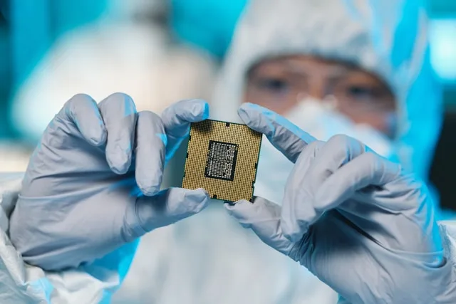
Jiangning Economic and Technological Development Zone holds Nanjing's most advanced logic fabrication capacity. TSMC's Fab 16 produces at the 16 nm and 28 nm nodes, employing approximately 2,800 people as of 2024. UMC operates an 8-inch facility in the same zone focused on embedded memory and power management ICs. NARI Technology, the State Grid subsidiary with roughly 11,000 employees, is headquartered here as well, producing IGBT modules and optical current transformers for smart grid applications.
This concentration makes Jiangning the centre of gravity for process engineering, yield management, and fab operations talent. It also makes it the primary target for competitor poaching.
Pukou and Jiangbei: The Compound Semiconductor Frontier
Pukou District is emerging as Nanjing's compound semiconductor hub. Sanan Optoelectronics brought its SiC wafer fab online in 2024 with an initial 200-person technical staff. Jiangbei New Area, which secured the RMB 42 billion investment package, hosts optical communication component manufacturers and materials firms supporting the broader IC supply chain.
The talent requirements in these districts skew toward SiC and GaN device engineering, MOCVD reactor operation, and compound semiconductor epitaxy. These are among the scarcest skill sets in China's semiconductor market.
Xingang and the Materials Spine
Xingang, within the Nanjing Economic and Technological Development Zone, houses Tongfu Microelectronics' advanced packaging facilities. Tongfu maintains roughly 25 billion units of annual capacity globally, with Nanjing operations representing approximately 30 percent of revenue. Nanjing Chemical Industry Park in Liuhe District provides the materials backbone: Entegris supplies chemical delivery systems, Linde provides specialty gases, and a cluster of domestic photoresist and wet chemical producers serve the Jiangning fabs.
The geographic spread matters for hiring because each district generates demand for overlapping but distinct skill profiles. A talent mapping exercise that treats "Nanjing semiconductor talent" as a single pool will miss the reality that a SiC device engineer in Pukou and a yield enhancement specialist in Jiangning occupy entirely different labour markets, even though they work 30 kilometres apart.
The Knowledge Drain That Capital Cannot Fix
Here is the analytical claim at the centre of this article, and it is one that investment figures alone will not reveal: Nanjing's expansion is not a capacity problem. It is a knowledge-transfer problem. The capital has arrived faster than the institutional knowledge required to use it can be replicated or retained.
TSMC Nanjing's 16 nm line carries years of embedded process knowledge in the engineers who ramped it. That knowledge is precisely what domestic competitors want. According to Nikkei Asia's October 2024 reporting, Hua Hong Semiconductor recruited senior process integration engineers from TSMC Nanjing at salary premiums of 40 to 50 percent, with signing bonuses equivalent to 8 to 12 months' salary. The Commercial Times in Taiwan reported that TSMC Nanjing responded with retention bonuses of RMB 200,000 to 500,000 per employee for critical 28 nm personnel.
The expansion to add 40,000 wafers per month at the 28 nm node depends on transferring yield ramp knowledge from the existing workforce to a new production line. If the engineers who hold that knowledge leave before the transfer is complete, the expansion does not simply slow. It produces wafers at lower yields, higher costs, and reduced competitiveness. The money has been spent. The building has been built. The knowledge required to make it productive walks out the door in the form of individual engineers, and no amount of capital expenditure can replace what they carry.
This is the dynamic that makes Nanjing's executive hiring challenge different from a generic talent shortage. The shortage is not merely of warm bodies with the right degree. It is of specific process knowledge that exists in a finite number of people, most of whom are already employed, and many of whom are being actively courted by competitors willing to pay 40 to 50 percent more to acquire what they know.
What the Roles Pay and Why the Gaps Persist
Compensation data for Nanjing's semiconductor cluster reveals a market that pays well by Jiangsu Province standards but persistently trails Shanghai, where the concentration of fabless design houses and venture-backed startups offers both higher cash compensation and equity upside that Nanjing's fab-dominated ecosystem cannot match.
Frontend Manufacturing and Process Engineering
A Senior Process Integration Engineer with 5 to 8 years of experience commands RMB 800,000 to 1,400,000 in Nanjing. That figure sits roughly 15 percent above the Jiangsu provincial median but 20 percent below Shanghai equivalents. The gap widens dramatically at the executive level. A VP of Fab Operations or Plant Manager with 12-plus years and 300mm fab experience earns RMB 2,500,000 to 4,500,000 in Nanjing, which represents 10 to 15 percent less than Shanghai. Equity participation is rare in Nanjing's fab-centric employment model, a structural disadvantage when competing against Shanghai's fabless unicorns where stock options form a material portion of total compensation.
Compound Semiconductors: Scarcity Pricing
The compound semiconductor segment tells a starker story. SiC device engineers specialising in MOSFET design earn RMB 900,000 to 1,600,000 in Nanjing. This is a severe shortage market. According to the China Semiconductor Industry Association's 2024 Talent Gap Analysis, approximately 80 percent of qualified compound semiconductor device engineers are passive candidates. They are not looking. They are not on job boards. They are not responding to postings.
At the executive level, a Chief Technology Officer in power electronics or optoelectronics commands RMB 3,000,000 to 5,500,000, with a premium attached to candidates who carry State Grid or NARI backgrounds that satisfy domestic verification requirements for power grid procurement.
Advanced Packaging: The Emerging Premium
Advanced Packaging R&D Managers with expertise in Fan-Out Wafer Level Packaging or 2.5D/3D architectures earn RMB 700,000 to 1,200,000 at firms like Tongfu Microelectronics. VP Engineering roles in outsourced semiconductor assembly and test operations reach RMB 1,800,000 to 3,200,000, but stock option availability remains limited compared to design houses. This compensation ceiling creates a retention challenge for packaging specialists who see greater financial upside in Shanghai's fabless ecosystem.
The compensation data points to a consistent pattern. Nanjing pays enough to attract junior talent but not enough to hold onto experienced specialists once they reach the seniority level where they become most valuable to competitors. The market is not underpaying in absolute terms. It is underpaying relative to the alternatives available to the specific individuals it most needs to keep.
Three Competing Cities and the Brain Drain Beneath the Surface
Nanjing does not compete for semiconductor talent in isolation. Three cities exert gravitational pull on the same candidate pool, each applying a different force.
Shanghai: The Prestige and Equity Gap
Shanghai's Zhangjiang Hi-Tech Park concentrates China's densest cluster of fabless design houses, EDA companies, and venture-backed semiconductor startups. Senior device physicists and fab directors can earn 30 to 40 percent more than Nanjing equivalents, with equity participation that Nanjing's state-adjacent employers rarely offer. For Taiwanese and overseas Chinese engineers, Shanghai provides superior international schooling and expatriate infrastructure. The competition is not purely about salary. It is about career trajectory, lifestyle infrastructure, and the perception that Shanghai sits closer to the centre of China's chip design future.
Suzhou: The Livability Arbitrage
Suzhou Industrial Park competes directly for process technicians and packaging engineers. Compensation levels are comparable to Nanjing, but housing costs are lower. According to the Suzhou Industrial Park Human Resources Development Report for 2024, equipment engineer turnover rates in Suzhou run 20 percent lower than Nanjing's. The implication is clear: when two cities offer similar pay, the one with a lower cost of living wins on retention. Nanjing's median housing price in Jiangning District reached RMB 28,000 per square metre, rising 8 percent annually, while entry-level fab technician salaries of RMB 90,000 to 120,000 per year lag further behind affordability benchmarks with each passing quarter.
Hefei: The Graduate Pipeline Diversion
The most recent competitive threat comes from Hefei, where CXMT's memory operations and NIO's semiconductor units are drawing digital design talent from Nanjing's universities with aggressive equity participation and government housing subsidies. According to the 21st Century Business Herald, this dynamic was already visible by early 2025, creating what the publication described as a brain drain of junior IC designers who might previously have entered Nanjing's fab pipeline.
This three-front competition means that Nanjing must fight to attract senior talent from Shanghai (where pay and prestige are higher), retain mid-career specialists against Suzhou (where quality of life is more affordable), and prevent its own university graduates from leaving for Hefei (where equity and housing incentives are more generous). No single compensation adjustment addresses all three fronts simultaneously. The response requires a different approach to identifying and engaging candidates who are not looking to move but might move for the right proposition.
Export Controls, Carbon Targets, and Water: The Regulatory Overlay
The talent challenge in Nanjing's semiconductor cluster does not exist in a vacuum. It sits inside a regulatory environment that constrains expansion, raises operating costs, and adds compliance complexity to every hiring decision.
U.S. Export Controls and the License Uncertainty
Current BIS restrictions limit Nanjing's access to EUV spare parts and certain etching equipment software updates. According to Reuters, Applied Materials and Lam Research paused new installations at the 16 nm line in 2024 pending BIS licence clarifications. The licenses governing EUV maintenance at Nanjing's advanced nodes expire in Q4 2025. Nikkei Asia reported in January 2025 that renewal uncertainty could delay the 28 nm expansion timeline.
For hiring leaders, this creates a paradox. The expansion requires engineers now. The expansion timeline itself depends on a regulatory decision that has not been made. Organisations that wait for clarity before hiring will find the candidates they need have already been recruited by competitors who moved earlier. Organisations that hire proactively accept the risk that timelines may shift but position themselves to execute the moment regulatory conditions permit.
Carbon and Water Constraints
Jiangsu's "Dual Carbon" targets mandate a 15 percent reduction in carbon intensity per unit of industrial output by 2026. Fabs face rising costs for captive solar installation or carbon credit purchases, estimated at RMB 0.08 to 0.12 per kilowatt-hour premium. Separately, Nanjing's allocation of Yangtze River water rights is capped at 3.5 billion cubic metres per year for industrial use. New fab expansions beyond 2026 will require water recycling rates exceeding 95 percent, up from the current 85 to 90 percent range.
These constraints do not directly affect hiring volumes, but they indirectly reshape the talent profile. Environmental compliance, sustainability engineering, and utility optimisation are becoming required competencies within fab operations teams, not optional add-ons. The executive search requirements for leadership roles in this market increasingly include regulatory fluency alongside traditional process engineering expertise.
Domestic Content and Verification
China's "New Infrastructure" procurement policies require domestic verification for silicon content in power grid projects. This benefits NARI and its supply chain but creates compliance burdens for foreign-joint-venture fabs seeking to supply State Grid. For hiring, this means that candidates with experience operating within State Grid's supplier qualification framework carry a premium that is difficult to replicate through training alone. The knowledge of how to satisfy these requirements is institutional and relationship-dependent.
Where Traditional Recruitment Fails in This Market
The passive candidate ratios in Nanjing's semiconductor cluster render conventional recruitment methods structurally inadequate for the most critical roles.
At the senior process integration engineer level, approximately 85 percent of qualified candidates are passive, according to the Hays Asia Salary Guide 2025. For Fab Operations Directors and VPs, the figure exceeds 90 percent, with average tenure in current roles exceeding four years. For compound semiconductor device engineers, 80 percent are passive due to extreme scarcity. These are not candidates who will respond to a job posting, no matter how well written or widely distributed.
The failure mode is predictable. An organisation posts a role. It receives applications from active candidates, who by definition represent the smaller, less experienced, or less settled portion of the market. The shortlist is assembled from this pool. The hiring manager finds the candidates underwhelming relative to the calibre required. The search restarts. Meanwhile, 112 days pass, as TSMC Nanjing's own yield enhancement engineer search demonstrated.
The candidates who will actually succeed in these roles are solving problems at their current employers. They are not browsing job boards. They are not updating their profiles on 51job.com. They are not attending career fairs. Reaching them requires direct headhunting methodology that identifies specific individuals based on their technical capabilities, maps their current compensation, assesses their mobility conditions, and approaches them with a proposition calibrated to what it would take to move them.
This is not a marginal improvement over job advertising. It is a fundamentally different method applied to a market where the conventional method has a structural ceiling. The 85 percent of senior candidates who are passive represent the talent that determines whether a billion-dollar fab expansion meets its yield targets or falls short. The 15 percent who are actively looking cannot carry that weight alone.
The cost of a failed search at this level is not measured in recruiter fees. It is measured in delayed production ramps, lower yields, and the competitive window that closes while the position remains vacant. The financial impact of a wrong or delayed executive hire in a semiconductor fab environment is orders of magnitude higher than in industries where the consequences of an empty seat accumulate slowly.
What Hiring Leaders in Nanjing Must Do Differently
The organisations that will secure the talent they need in this market share three characteristics. They move before the role is formally open. They compete on proposition, not just compensation. And they use methods designed for passive markets rather than active ones.
Moving early means building relationships with potential hires before a vacancy exists. In a market where senior process integration engineers take 112 days to fill, the organisation that began its search 90 days before the vacancy had a candidate identified and engaged before competitors knew the role existed. Proactive talent pipeline development is not a luxury in Nanjing's semiconductor market. It is a prerequisite for timely hiring.
Competing on proposition means understanding that a 40 to 50 percent salary premium is only one lever. The engineers being poached from TSMC Nanjing are not moving purely for money. They are moving because the domestic competitors offer faster career progression, broader technical scope, and, in some cases, the chance to build a process from scratch rather than operate an established one. A compelling proposition addresses the professional ambition, not just the bank account.
Using methods designed for passive markets means engaging an executive search partner with the methodology and market intelligence to identify, assess, and approach the specific individuals who hold the knowledge your expansion requires. In a market where 85 to 90 percent of senior candidates are not looking, the difference between a search that reaches those candidates and one that does not is the difference between a successful hire and a re-listed role.
KiTalent delivers interview-ready executive candidates within 7 to 10 days through AI-enhanced direct headhunting, with full pipeline transparency and a pay-per-interview model that eliminates upfront retainer risk. With a 96 percent one-year retention rate across 1,450-plus completed placements, KiTalent's approach is built for exactly the kind of passive, specialised market that Nanjing's semiconductor cluster represents.
For organisations expanding fabrication, packaging, or compound semiconductor capacity in Nanjing and competing for the engineers and leaders who will determine whether that investment produces results, speak with our executive search team about how we identify and engage candidates in markets where conventional methods reach fewer than 15 percent of the viable pool.
Frequently Asked Questions
What semiconductor roles are hardest to fill in Nanjing in 2026?
Senior Yield Enhancement Engineers with 28 nm node expertise, Fab Operations Directors with 300mm experience, and SiC/GaN device engineers are the most difficult roles to fill. Yield enhancement engineer searches at TSMC Nanjing averaged 112 days in late 2024, nearly three times the fill time for equivalent roles in Shanghai. The passive candidate rate for these roles ranges from 80 to 90 percent, meaning the vast majority of qualified professionals are not actively seeking new positions and cannot be reached through job postings or recruitment advertising.
How does Nanjing semiconductor compensation compare to Shanghai?
Senior Process Integration Engineers in Nanjing earn RMB 800,000 to 1,400,000, approximately 20 percent below Shanghai equivalents. VP of Fab Operations roles command RMB 2,500,000 to 4,500,000, roughly 10 to 15 percent below Shanghai. The gap widens further when equity is included, as Shanghai's fabless design house ecosystem offers stock options that Nanjing's fab-dominated employers rarely provide. This compensation differential drives talent migration toward Shanghai, particularly at the senior specialist and executive levels.
What is driving the semiconductor talent shortage in Nanjing?
Three forces converge. First, multi-billion-dollar capacity expansions by TSMC and others are creating simultaneous demand for experienced engineers. Second, domestic competitors are poaching senior talent at 40 to 50 percent salary premiums. Third, Nanjing's 5,000 annual microelectronics graduates lack the specific cleanroom operating skills fabs require, creating a 30 to 40 percent gap between academic output and operational demand. KiTalent's direct headhunting methodology addresses this by identifying passive specialists who hold the process knowledge these expansions require.
How do U.S. export controls affect semiconductor hiring in Nanjing?
BIS export controls restrict access to EUV spare parts and certain equipment software updates at Nanjing's advanced nodes. Licence expiry in late 2025 created uncertainty around the 28 nm expansion timeline. For hiring leaders, this produces a paradox: the expansion requires engineers now, but the expansion schedule depends on regulatory decisions not yet finalised. Organisations that delay hiring until regulatory clarity arrives find that candidates have already accepted offers from competitors who moved earlier.
Why does executive search outperform job advertising for semiconductor roles in Nanjing?
Job advertising reaches only active candidates, who represent 10 to 20 percent of the qualified pool for senior semiconductor roles in Nanjing. The remaining 80 to 90 percent are passive professionals embedded in current positions. KiTalent's AI-enhanced talent mapping identifies these individuals by technical capability, compensation profile, and mobility conditions, then approaches them directly with propositions calibrated to their specific circumstances. This is why executive search consistently outperforms advertising in markets defined by passive candidate dominance.
What should organisations consider when hiring compound semiconductor engineers in Nanjing?
The compound semiconductor talent market in Nanjing is extremely small. Sanan Optoelectronics' Pukou fab launched with only 200 technical staff. Roughly 80 percent of qualified SiC and GaN device engineers are passive. Compensation for SiC MOSFET design specialists ranges from RMB 900,000 to 1,600,000, but salary alone rarely moves these candidates. Organisations must compete on technical scope, career trajectory, and the calibre of the problems candidates will solve. Proactive succession and pipeline planning is essential given the lead times involved.