Phoenix Semiconductor Hiring: $65 Billion in Capital, and a Talent Deficit That Money Cannot Close

Phoenix entered 2026 as the most heavily capitalised semiconductor manufacturing corridor in the Western Hemisphere. TSMC's $65 billion gigafab campus in north Phoenix began production in early 2025. Intel's Ocotillo complex in Chandler maintains over 12,000 employees and secured $8.5 billion in direct CHIPS Act funding. Fourteen Tier-1 suppliers have established local operations. The physical infrastructure for a world-class chip manufacturing cluster is either built or under construction.
The workforce to operate that infrastructure is not. The Phoenix metro faces an annual deficit of 3,000 to 4,000 qualified semiconductor professionals against current demand. TSMC's production ramp has slipped 12 to 18 months from original targets, and the root cause is not equipment, permitting, or water. It is the inability to hire and retain the engineers who make advanced node fabrication work. Senior EUV equipment engineers sit vacant for 120 to 150 days. Process integration roles at 3nm and 2nm nodes require experience that fewer than a few hundred professionals in the United States possess. The capital moved faster than the human capital could follow.
What follows is an analysis of how this gap formed, where it is most acute, and what it means for the organisations trying to build and operate the facilities that define Phoenix's semiconductor future. The data covers compensation, competition from rival markets, passive candidate dynamics, and the systemic constraints that make traditional hiring methods inadequate for this specific market.
The Silicon Desert Is Real. Its Workforce Is Not Ready.
The term "Silicon Desert" is no longer aspirational branding. The Greater Phoenix Economic Council and Arizona Commerce Authority deploy it in formal materials, and the cluster supporting that label now includes every tier of the semiconductor value chain. TSMC's three-phase Fab 21 campus anchors the north. Intel's Ocotillo campus anchors the southeast. ON Semiconductor, NXP Semiconductors, and Microchip Technology operate fabrication and design facilities across the East Valley. Applied Materials maintains its Tempe headquarters. ASM International is headquartered in Scottsdale. Amkor Technology runs advanced packaging operations from Tempe. ASML and LAM Research have established service operations to support the EUV lithography and etch tools inside the fabs.
This density matters because semiconductor manufacturing depends on ecosystem proximity. A fab does not operate in isolation. It requires chemical suppliers within hours, equipment service engineers within minutes, and a labour pool deep enough to absorb the cyclical hiring surges that accompany each new process node ramp. Phoenix now has the supplier density. It does not have the labour depth.
The metro anticipates 4,500 to 6,000 new direct semiconductor manufacturing jobs by the end of 2026, with a three-to-one multiplier effect for indirect employment. Against that demand, the annual structural deficit of 3,000 to 4,000 qualified professionals means the market is falling further behind with each quarter. Arizona State University's Fulton Schools of Engineering produces over 5,000 engineering graduates annually, and the Maricopa Community Colleges "Quick Start" programme certifies roughly 500 semiconductor technicians per year. These are meaningful numbers. They are not sufficient for the scale of hiring underway.
The gap between what the education pipeline produces and what the fabs require is not a volume problem alone. It is a specificity problem. And that distinction drives every hiring challenge a Phoenix-area semiconductor employer faces in 2026.
Capital Arrived in 2024. Talent Did Not Follow on the Same Timeline.
TSMC announced its escalated $65 billion commitment in April 2024. Of that figure, $35 billion had been deployed by the end of the year. Phase 1 entered production in Q1 2025 with 4nm process technology. Phase 2 is now in critical equipment move-in stages, targeting 3nm and 2nm processes. Phase 3, announced alongside the total investment figure, will add further 2nm capacity.
Intel secured $8.5 billion in direct CHIPS Act funding plus up to $11 billion in federal loans in March 2024, according to the U.S. Department of Commerce CHIPS Program Office. Arizona was designated as a primary beneficiary for advanced packaging and logic manufacturing. The company's 2026 trajectory hinges on its Intel 18A foundry process development, which is centred at the Ocotillo campus.
The capital commitment is the largest in Arizona's economic history. The timeline slippage is the largest operational embarrassment the state's semiconductor ambitions have faced.
Why Production Ramps Slip When Buildings Are Finished
TSMC's production ramp to full volume faces a 12 to 18 month delay from original 2024 targets, according to supply chain reporting by Nikkei Asia. The buildings exist. The clean rooms are built. The delay is workforce readiness: the engineers who install, calibrate, qualify, and operate advanced node equipment were not available in the Phoenix labour market at the volume and specificity required.
This is the core analytical tension of Phoenix's semiconductor story in 2026. Capital deployment velocity has outstripped human capital formation by a margin so wide that a $65 billion investment could not buy its way to an on-time production start. The political narrative of a "manufacturing renaissance" is technically accurate in terms of physical plant. It is operationally incomplete because production readiness requires a workforce that the market has not yet assembled.
The implications cascade beyond TSMC. Phase 2 will require 6,000 construction workers and 2,000 additional operational staff. The supplier ecosystem surrounding the campus is scaling in parallel, each firm competing for the same constrained talent pool. Every new supplier facility that opens in the metro adds demand without meaningfully adding supply.
The Roles Where the Deficit Is Most Acute
Not all semiconductor roles are equally hard to fill. The deficit concentrates in four categories where the required experience is both highly specific and extremely scarce.
Process Integration and Yield Engineering
Process integration engineers with advanced node experience at 3nm and 2nm represent the single most constrained talent category in the Phoenix market. According to LinkedIn Talent Insights and SIA data, 85% of qualified candidates at the senior level are passive. They are employed, not looking, and in roles where their knowledge is critical to their current employer's production output.
Yield engineers are characterised as "super passive" in industry workforce analyses, with average tenure of 5.2 years in a single role. Seventy percent of hires in this category come from direct recruiting or internal referrals rather than applications. The implications for any organisation relying on job postings to fill these roles are straightforward: the method reaches fewer than a third of the viable candidates.
A Director of Process Integration in Phoenix commands a base salary of $280,000 to $350,000. The role is critical for advanced node ramp and there is no apprenticeship path. The knowledge required comes from years of hands-on experience with specific process nodes. You cannot recruit experience that does not yet exist in sufficient quantity in this geography.
EUV Lithography and Equipment Specialists
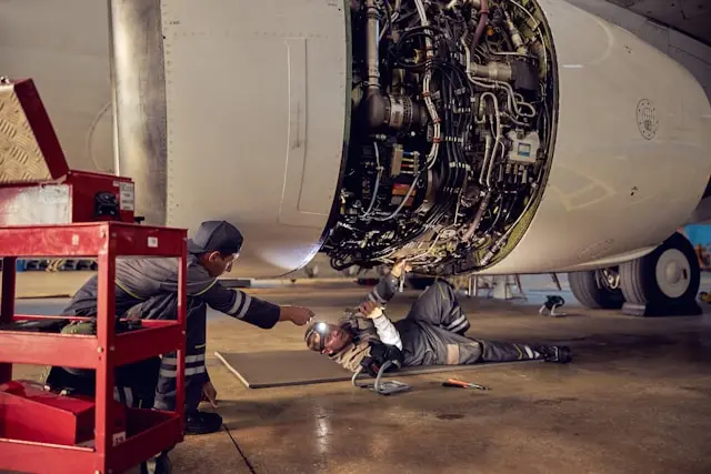
EUV lithography specialists represent the sharpest point of the talent deficit. The active candidate pool contains only 20 to 25 percent of viable talent. The remainder must be recruited from ASML, Nikon, or Canon service organisations via direct headhunting methods. Senior field service engineers for EUV lithography and advanced etch equipment experience typical vacancy durations of 120 to 150 days in the Phoenix metro, compared to 60 to 75 days in the Bay Area.
That comparison is counterintuitive. Phoenix, with its lower cost of living and new facilities, should in theory be easier to hire for than the saturated Bay Area market. It is harder. The reason: the Bay Area has the installed base of experienced professionals. Phoenix is building demand before supply has migrated. One major equipment supplier has reportedly offered $25,000 signing bonuses for senior technicians with specific Applied Materials or Lam Research tool experience, a figure that signals desperation rather than standard recruitment practice.
The cost of unfilled equipment engineer roles is not abstract. Fabs require 99.9999% uptime. Power quality events alone cost $10 to $20 million per incident in lost wafer production. An equipment engineer vacancy does not simply delay a hire. It delays production, destroys yield, and compounds costs across the entire operation.
TSMC's Structural Adaptation: Importing What It Cannot Hire
The most telling signal of Phoenix's talent deficit is not a vacancy statistic. It is TSMC's decision to import rather than hire locally.
According to U.S. Department of Labor H-1B and L-1 visa disclosure data, and as reported by Reuters in December 2023, TSMC filed visa petitions for approximately 500 Taiwanese engineers and technicians for the Arizona facility. The roles included process integration engineers, yield engineers, and EUV equipment specialists. The stated rationale was the inability to source local talent with advanced node experience.
This is not a standard foreign worker strategy. It is a structural adaptation by the market's anchor tenant. TSMC did not supplement local hiring with international talent. It replaced a local hiring strategy that had failed with an international one, accepting the delays of visa processing as a lesser cost than continued vacancies.
The visa system itself introduces further constraint. H-1B annual caps of 65,000 (plus 20,000 advanced degree exemptions) limit transfer volume. Processing delays of six to nine months for employment-based green cards create retention uncertainty. An engineer brought to Phoenix on a visa petition may have the skills and the willingness. The immigration system may not have the capacity.
Intel, facing the same talent competition from a different direction, responded with retention rather than importation. According to industry analyst reports and compensation data, Intel's Ocotillo campus implemented retention bonuses of 30 to 50 percent of base salary for senior process engineers with five or more years of experience during 2023 and 2024. The trigger, according to these reports, was the risk of losing experienced engineers to competitors entering the same market. This represents a cost increase that was not initially budgeted in CHIPS Act workforce projections.
The two strategies highlight the same underlying problem. One employer imported because it could not hire. The other paid retention premiums because it could not afford to lose. Both responses are expensive. Neither is sustainable at current scale.
Compensation: Competitive Nationally, Outgunned by Headquarters Markets
Phoenix semiconductor compensation tells a split story. The market offers 15 to 20 percent salary premiums over the national average for equivalent roles. When adjusted for cost of living, Phoenix competes favourably with Austin. At the senior specialist and management level, the numbers are credible: senior process engineers earn $145,000 to $175,000 in base salary, reaching $200,000 with bonuses. Fab operations managers command $160,000 to $200,000. Senior equipment engineers earn $135,000 to $165,000, with a 15 percent premium for those holding specific Applied Materials or Lam Research tool expertise.
At the executive level, the packages are substantial. A VP of Fab Operations or Plant Manager in Phoenix earns $350,000 to $500,000 in base salary. Total compensation including equity and performance bonuses reaches $600,000 to $900,000. A VP of Supply Chain, a role increasingly critical as the localisation requirement deepens, commands $250,000 to $320,000 in base.
The problem is not that Phoenix pays poorly. The problem is that Phoenix competes for the same people as markets that pay more and offer something Phoenix cannot match: headquarters career trajectory.
The Bay Area Premium and Its Gravitational Pull
San Jose and the broader Bay Area remain home to Applied Materials, Lam Research, and KLA headquarters. These employers offer 25 to 30 percent compensation premiums for equivalent roles and provide career paths to corporate leadership functions that do not exist in a satellite manufacturing campus. Director-level professionals and above are drawn to the Bay Area despite its higher cost of living because the equity appreciation potential and the career ceiling are both higher.
A senior process engineer in Phoenix may earn $175,000 in base salary and $200,000 in total compensation. The equivalent role in San Jose may offer $225,000 in base and $280,000 in total, plus restricted stock in a publicly traded equipment company whose valuation is tied to the very capacity expansion Phoenix is undertaking. The candidate knows this. The recruiter offering a Phoenix role needs to compete not just on salary but on a career proposition that addresses long-term trajectory.
Austin: The No-Tax Rival
Austin is Phoenix's primary competitor for fab engineering talent. Samsung's $25 billion Taylor fab and established operations from NXP, Infineon, and Texas Instruments create direct competition for the same process and yield engineers. Austin offers comparable base salaries with no state income tax and marginally lower median home prices: $420,000 compared to Phoenix's $450,000. For a candidate weighing two offers, the after-tax difference in disposable income favours Austin materially.
Phoenix's cost of living advantage over the Bay Area is real and well understood. Its disadvantage relative to Austin on tax treatment is less discussed and equally relevant. A candidate earning $175,000 in Phoenix pays Arizona state income tax. The same candidate earning the same amount in Austin does not. Over a career, the difference compounds.
The Systemic Constraints That Compound the Hiring Challenge
The talent deficit does not exist in isolation. It sits within a broader set of systemic constraints that amplify hiring difficulty and limit the strategies available to employers.
Housing affordability has deteriorated. The median home price in Phoenix reached $450,000, with average rents of $1,850 for a one-bedroom unit. For candidates recruited from lower-cost Midwest and Southern markets, the relocation calculation is not straightforward. A technician earning $75,000 in a market where housing costs $250,000 faces a meaningful reduction in purchasing power when moved to Phoenix, even with a 15 percent salary increase.
Industrial real estate adds a second layer of constraint. Class A manufacturing vacancy in the metro is below 3 percent, restricting supplier expansion at exactly the moment the ecosystem requires it. A Tier-1 chemical supplier ready to open a Phoenix facility to serve TSMC may find the site before it finds the workforce, or may find the workforce before the site. Rarely both simultaneously.
Environmental permitting creates 12 to 18 month lead times for fab expansion. The Arizona Department of Environmental Quality regulates hazardous waste from dopants including arsenic and phosphine. The EPA's "Good Neighbour" rule implementation in 2024 added compliance costs for emissions control. These timelines cannot be shortened with capital. They can only be planned around, and that planning requires the environmental, health, and safety specialists who are themselves in short supply.
Grid stability is a less visible but operationally critical concern. Arizona Public Service and Salt River Project have committed $500 million in grid infrastructure upgrades to support the TSMC campus. Summer peak load constraints from June through September present specific operational risks. A senior facilities engineering leader responsible for fab uptime in Phoenix must manage power quality to a standard of 99.9999 percent availability, in a region where summer demand strains the grid annually.
Water: The Risk That Is Not What It Appears
Public perception of Phoenix semiconductor manufacturing is shaped by a single narrative: "building chip fabs in the desert." The water story is more nuanced than the headline suggests.
TSMC and Intel utilise reclaimed water from the City of Phoenix's 91st Avenue Wastewater Treatment Plant. Both companies achieve over 90 percent recycling rates through zero-liquid discharge systems. Each fab requires 2 to 4 million gallons daily. Both companies hold 100-year assured water supply certificates under Arizona law.
The legal reality is that semiconductor firms have secured industrial water allocations that extend to 2080. The physical reality is that Arizona's Tier 1 drought status and mandatory Colorado River cutbacks affect agricultural and residential users, not industrial certificate holders. The political reality is the space between those two facts.
If prolonged drought intensifies residential water restrictions while industrial fabs continue operating on legally assured allocations, the "water for chips" trade-off becomes a political flashpoint. This is not an operational risk in 2026. It is a regulatory and reputational risk on a longer horizon. For hiring leaders, the immediate implication is simpler: candidates read headlines about Arizona drought. The perception of water risk is itself a recruitment barrier, even when the operational risk is managed. Addressing that perception during the candidate engagement and negotiation process is now part of the search strategy for any senior hire relocating to Phoenix.
What This Means for Hiring Leaders in 2026
The Phoenix semiconductor talent market in 2026 requires a fundamentally different approach to executive and specialist hiring than what most organisations have used historically. The reasons are specific and data-driven.
Eighty-five percent of senior process integration engineers are passive. Seventy percent of yield engineer hires come through direct sourcing, not applications. EUV lithography specialists are only 20 to 25 percent addressable through active channels. A traditional search approach built on job advertising and inbound applications reaches, at best, one-quarter of the viable talent pool for the most critical roles.
The competitive dynamics compound the problem. Austin, San Jose, Hillsboro, and Hsinchu all compete for the same profiles. Intel and TSMC compete within the same metro. The supplier ecosystem competes with its own customers for the same engineers. A candidate with EUV tool experience and a current Phoenix address receives multiple approaches per month. The time between a candidate becoming available and a candidate accepting an offer has compressed to the point where a 120-day search process means losing every first-choice candidate.
The approach that works in this market combines three elements. First, proactive talent mapping that identifies and assesses passive candidates before a vacancy opens. Second, speed: the window between identifying a candidate and presenting an offer must compress from months to weeks. Third, market intelligence on compensation, competitor activity, and candidate motivation that allows the hiring organisation to construct an offer the candidate cannot find elsewhere.
KiTalent's approach to executive search in the semiconductor and advanced technology sector is built around these requirements. Interview-ready candidates delivered within 7 to 10 days. A pay-per-interview model that eliminates upfront retainer risk. AI-powered talent mapping that reaches the passive majority that no job board surfaces. Across 1,450 executive placements with a 96% one-year retention rate, the methodology is designed for exactly the conditions Phoenix's semiconductor market now presents.
For organisations competing to hire the process engineers, equipment specialists, and operations leaders who will determine whether Phoenix's semiconductor ambitions become production reality, the cost of a slow or poorly targeted search is not a delayed start date. It is a production delay measured in millions of dollars per week. Open a conversation with our executive search team about how to reach the candidates this market requires.
Frequently Asked Questions
What is the salary range for senior semiconductor engineers in Phoenix in 2026?
Senior process engineers in the Phoenix metro earn $145,000 to $175,000 in base salary, reaching $160,000 to $200,000 with bonuses. Senior equipment engineers earn $135,000 to $165,000, with a 15% premium for those holding specific tool platform expertise. At the executive level, a VP of Fab Operations commands $350,000 to $500,000 in base, with total compensation reaching $600,000 to $900,000 including equity and performance incentives. Phoenix offers 15 to 20% premiums over the national average but sits 10 to 15% below Austin and 25 to 30% below San Jose for equivalent roles. Firms seeking accurate compensation benchmarking for semiconductor roles should engage specialist advisors with current market data.
Why is TSMC's Phoenix fab behind schedule?
TSMC's production ramp to full volume at Fab 21 has slipped 12 to 18 months from original targets. The delay is not attributable to construction, equipment, or permitting. It is a workforce readiness gap. The advanced node processes TSMC is bringing to Phoenix, including 3nm and 2nm technology, require engineers with specific experience that the local labour market does not contain in sufficient volume. TSMC filed approximately 500 visa petitions for Taiwanese engineers and technicians to address the shortfall, indicating that local sourcing strategies could not meet the timeline. Phase 2 equipment move-in, now underway, will add further hiring pressure through 2026 and 2027.
How many semiconductor jobs will Phoenix add by the end of 2026?
The Phoenix metro anticipates 4,500 to 6,000 new direct semiconductor manufacturing jobs by the end of 2026, according to Arizona Office of Economic Opportunity projections. These direct roles carry a three-to-one multiplier for indirect employment, meaning the total economic impact includes 13,500 to 18,000 additional positions across the supply chain, services, and supporting industries. Against this demand, the metro faces a structural annual deficit of 3,000 to 4,000 qualified semiconductor professionals. ASU produces over 5,000 engineering graduates annually and Maricopa Community Colleges certify roughly 500 semiconductor technicians per year, but the specificity of skills required outpaces the pipeline's output.
What makes semiconductor hiring in Phoenix different from other tech markets?
Phoenix's semiconductor market is distinctive because it is scaling from near-zero advanced manufacturing capacity to the most concentrated fab cluster in the Western Hemisphere within a five-year window. Unlike the Bay Area or Austin, which have decades-deep installed talent bases, Phoenix is creating demand before supply has migrated. This means passive candidate ratios are higher, vacancy durations are longer, and the competition for experienced engineers is intensified by the simultaneous scaling of multiple employers in the same geography. KiTalent's direct search methodology is designed for markets where the majority of qualified candidates are not visible through conventional channels.
Is water scarcity a real risk for Phoenix semiconductor manufacturing?
The operational water risk for semiconductor fabs in Phoenix is currently managed rather than acute. TSMC and Intel hold 100-year assured water supply certificates under Arizona law, utilise reclaimed water from municipal treatment facilities, and achieve over 90% recycling rates through zero-liquid discharge systems. The longer-term risk is political rather than hydrological: if prolonged drought intensifies residential water restrictions while industrial fabs continue operating on legally secured allocations, public and regulatory pressure could shift. For candidates evaluating relocation to Phoenix, addressing this perception gap is now a standard part of the recruitment conversation.
How long does it take to fill a senior semiconductor engineering role in Phoenix?
Senior equipment engineer vacancies in the Phoenix metro typically remain open for 120 to 150 days, compared to 60 to 75 days for comparable roles in the Bay Area. Process integration and yield engineering roles at the director level and above can run even longer due to the extreme specificity of required experience. For organisations that cannot afford four to five months of vacancy on a production-critical role, why conventional executive recruiting approaches often fail in constrained markets like this is worth understanding before launching a search.