Suwon's Electronics R&D Cluster in 2026: The Hiring Paradox Inside Samsung's Orbit
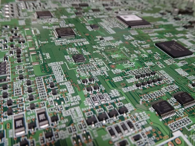
Samsung Electronics' Digital City complex in Suwon houses approximately 32,000 R&D personnel across 390,000 square metres of research facilities. It anchors one of the highest concentrations of consumer electronics and semiconductor design engineers on the planet. By every surface measure, this is a market with deep talent. The reality beneath that surface is considerably more complicated.
The complication is not a simple shortage. It is a splitting of the market into two distinct halves. One half, covering mature mobile device engineering and system integration, shows softening demand and conservative headcount management. The other half, covering sub-3nm process design, High Bandwidth Memory architecture, and AI semiconductor integration, is starved of qualified professionals to the point where roles sit unfilled for more than seven months. The same organisation, in the same campus, is simultaneously contracting and unable to hire. That paradox defines Suwon's talent market in 2026.
What follows is a ground-level analysis of why this bifurcation exists, what it means for the organisations competing inside Samsung's ecosystem, and why the hiring strategies that worked in this cluster five years ago no longer reach the candidates who matter most.
Samsung's Two Workforces: Efficiency and Scarcity in the Same Building
The public narrative around Samsung Electronics through 2024 centred on efficiency. Group-wide restructuring, hiring freezes in non-core divisions, and a 34% decline in operating profit in Q3 2023 created a market perception of workforce slack. Headlines suggested Samsung was trimming. The talent market responded accordingly: passive candidates assumed the environment was unfavourable, active applicants hesitated, and external observers concluded that Suwon's advanced electronics talent pool was loosening.
Internal recruitment data tells a different story. While the Mobile eXperience division held headcount flat and corporate functions contracted, the Device Solutions division's requisitions for AI chip architects and 3nm GAA transistor designers remained 40% unfilled against headcount plans through 2024. Average time-to-fill for these roles extended to 5.2 months. For the most specialised positions, such as Senior Process Integration Engineers with commercial Gate-All-Around production experience, that figure stretched to 7.5 months, nearly triple the 2.8-month average for general semiconductor engineering roles, according to Incruit Corp.'s semiconductor sector hiring analysis.
This is the analytical claim that sits at the centre of Suwon's talent story: the restructuring headlines created a false impression that qualified talent was available. The efficiency measures targeted administrative, commercial, and commodity engineering roles. The simultaneous shortage in the specialisms that determine Samsung's competitive position against TSMC and SK Hynix deepened during the same period. Any hiring leader reading the aggregate employment numbers and concluding that Suwon is an easier market to recruit in has misread the data entirely.
The Cluster That Built Suwon Is Now Fragmenting
Suwon's identity as Korea's premier electronics R&D hub rests on four decades of concentrated investment in advanced technology and semiconductor design. Digital City is not merely a large campus. It is the centre of gravity for an ecosystem of approximately 1,200 registered subcontractors and equipment suppliers operating within a 50-kilometre radius, with 340 firms maintaining offices specifically in Suwon's Yeongtong and Gwonseon districts.
The Pyeongtaek Migration
That gravity is now shifting. Samsung's announcement of KRW 60 trillion in domestic R&D investment for 2025 and 2026 allocated 70% of the total to the K-Semiconductor Mega Cluster spanning Pyeongtaek and Yongin, not Suwon. The relocation of approximately 800 Advanced Packaging Team personnel from Digital City to the new Pyeongtaek Giga-Fab complex in January 2024 was a visible signal of this redirection. According to Gyeonggi Provincial Government projections, Suwon's advanced electronics R&D employment will contract by 3 to 5% by late 2026, while Hwaseong and Pyeongtaek grow by 18% and Pangyo grows by 12%.
What Remains in Suwon
Digital City is transitioning toward mature node design, mobile system architecture, and AI-on-device software optimisation. These are valuable disciplines. They are also lower-margin and higher-volume activities increasingly vulnerable to competition from Chinese manufacturers. The most advanced semiconductor process R&D, the work that commands the highest talent premiums and the longest vacancy durations, is migrating to the K-Semiconductor Belt. What remains in Suwon is not weak. But it is no longer the strategic frontier.
For hiring leaders at Suwon-based suppliers, this geographic fragmentation creates a practical problem. The talent pipeline that once concentrated in a single district is now distributed across three locations separated by 40 to 80 kilometres of congested Gyeonggi Province highway. Candidates who once considered Digital City the obvious destination now weigh Pyeongtaek's newer facilities and Pangyo's superior urban amenities against Suwon's mature but increasingly repositioned cluster.
The Compensation Trap: Underpaying a Global Market
Suwon's compensation structure for semiconductor and device R&D professionals reflects Samsung Electronics' historically disciplined pay philosophy. A Senior Specialist or Manager with 12 to 18 years of experience earns KRW 120 to 180 million in base salary, with total compensation reaching KRW 150 to 220 million including performance bonuses, according to the HR Managers Association of Korea's 2024 Semiconductor Industry Compensation Survey. At Executive and VP level, base salaries range from KRW 280 to 450 million, with total packages including stock options reaching KRW 400 to 700 million.
These figures represent a 15 to 20% discount to equivalent roles at TSMC and MediaTek in Taiwan, and a 40 to 50% discount to Silicon Valley equivalents according to Radford's Global Technology Survey 2024. For a Senior Process Engineer, the U.S. market offers USD 180,000 to 250,000, equivalent to KRW 240 to 330 million, a level inaccessible anywhere in the Suwon market. TSMC offers Korean engineers total compensation packages of TWD 3 to 5 million annually, roughly double Samsung's rates for equivalent seniority, plus Mandarin language support.
The gap is not closing. It is widening fastest at exactly the seniority level where the most critical roles sit. The candidates Samsung needs most, those with commercial experience in GAA transistor architecture, HBM3E memory interface design, or 2.5D/3D chiplet integration, are the candidates most visible to international recruiters offering packages Suwon cannot match. According to The Chosun Ilbo's reporting in November 2024, SK Hynix recruited a team of six senior HBM design architects from Samsung's Suwon-based Memory Product Planning team during Q4 2024, offering compensation premiums of 40 to 60% above standard Samsung salary bands. Samsung responded with retention bonuses of KRW 50 to 100 million for remaining HBM specialists, an unusual defensive measure for the typically rigid Samsung compensation structure.
This creates a cascading problem. When Samsung matches a competitor's offer for one critical specialist, it creates internal equity pressure across the team. When it does not match, it loses a node of institutional knowledge that cannot be replaced by hiring a junior engineer and waiting eight years. Either path is expensive. Neither is sustainable.
Four Markets Competing for the Same 2,000 Professionals
The talent Suwon needs is not simply scarce in Suwon. It is scarce globally. Fewer than 2,000 professionals worldwide possess commercial GAA production experience. The competition for this pool is being waged simultaneously by four distinct geographic markets, each with different advantages.
Internal Gyeonggi Competition
Samsung's own Pyeongtaek and Yongin facilities are the most immediate competitors. Internal transfer policies disclosed in labour union filings show relocation packages and new facility incentives equivalent to 10 to 15% salary premiums for engineers willing to move from Suwon to the K-Semiconductor Belt. For engineers interested in process integration rather than pure design, the proximity to actual manufacturing lines at Pyeongtaek's P3 and P4 fabs is a genuine pull factor that Suwon's design-focused campus cannot replicate.
The Pangyo Premium
Fifteen kilometres northeast, Pangyo Techno Valley offers what Suwon struggles to provide: superior urban amenities, international schools, and a dense concentration of AI and fabless semiconductor startups. Companies including Rebellions, FuriosaAI, and Sapient offer cash compensation 20 to 30% above Samsung's bands for SoC architects. The trade-off is job security. But for a senior engineer who has spent 8.2 years at Samsung, the average tenure for these specialisations according to LinkedIn Talent Solutions' Korea Semiconductor Market Insights, the risk calculus on a well-funded startup begins to look different.
Taiwan and the United States
TSMC and MediaTek maintain active recruitment pipelines targeting Samsung's 3nm and memory design teams. The U.S. market, supercharged by CHIPS Act incentives, has created specific demand for bilingual Korean-English senior process engineers at Samsung's Austin fab expansion and across the wider semiconductor supply chain. These international competitors are not poaching at scale. They are extracting individual specialists whose departure creates disproportionate organisational impact.
For organisations hiring in this market, understanding where talent is moving and why is not optional intelligence. It is the prerequisite to any viable search strategy.
The Missing Middle and the Demographic Cliff
Suwon's talent scarcity is not only a demand-side problem. The supply pipeline is contracting at its foundation. Gyeonggi Province's 25 to 34 age cohort, the primary recruitment pool for R&D positions, declined by 12% between 2020 and 2025 according to Statistics Korea's population projections. Samsung Digital City's entry-level engineering hiring decreased 18% over the same five-year period despite increased demand for senior talent.
The result is what the data reveals as a "missing middle" in the experience pipeline. Samsung has deep benches of engineers with 15 or more years of tenure and a reduced but functional intake of fresh graduates. What it lacks is the mid-career cohort of 7 to 12 year professionals who would normally be stepping into senior technical leadership. These are the engineers who bridge the gap between theoretical knowledge and production-hardened expertise. Their absence means that when a senior specialist departs, the next candidate in the internal pipeline is often three to five years away from readiness.
Compounding this, the elimination of approximately 15% of Suwon's foreign technical workforce due to increasing restrictions on Chinese national engineers working in advanced semiconductor R&D has created sudden shortages in materials engineering roles. Positions previously filled by graduates of Peking University and Tsinghua University now sit open, and the domestic pipeline cannot absorb the gap at the volumes required.
The demographic trajectory does not reverse in 2026 or 2027. It steepens. Any organisation building a long-term talent acquisition strategy in this cluster must price in a structurally thinning supply of qualified entrants to the profession.
Why Conventional Search Fails in This Market
The market data on passive candidates in Suwon's advanced electronics sector is unambiguous. Approximately 85% of qualified candidates for senior SoC architecture, HBM circuit design, and 3nm process integration roles are currently employed and not actively applying to job postings. These professionals have an average tenure of 8.2 years at their current employer. They are not browsing job boards. They are not updating their CVs.
Job postings for Advanced Package Design and Mobile SoC Architecture roles in Suwon increased 34% year-on-year in Q1 2025. Over the same period, the applicant-to-position ratio for roles requiring 10 or more years of experience dropped to 0.8 to 1. Fewer than one qualified applicant per open role. Posting the position and waiting for inbound applications is not a viable strategy in a market structured this way.
The hidden 80% of passive talent in most executive markets becomes closer to 85% in Suwon's semiconductor specialisms. This is a market where the conventional search playbook, post the role, screen inbound applications, build a shortlist from respondents, systematically excludes the vast majority of viable candidates. The organisations that continue to rely on it are not just slower. They are searching in the wrong pool entirely.
What works in this market is direct identification and confidential approach. It requires mapping the specific teams at Samsung, SK Hynix, TSMC, and the Pangyo startups where the target candidates currently sit. It requires understanding the non-compete constraints that Korean courts now limit to 6 to 12 months following the 2023 Commercial Act revision. It requires building a proposition that addresses not just compensation but the specific career calculation a passive candidate makes when weighing Samsung's institutional scale against a startup's equity, or Suwon's mature cluster against Pyeongtaek's frontier facilities.
What Hiring Leaders in This Market Need to Do Differently
The Samsung dependency that defines Suwon's electronics cluster is both an advantage and a vulnerability for every employer operating within it. When Samsung hires aggressively, the entire ecosystem tightens. When Samsung contracts, the perception of talent availability misleads hiring leaders at every tier of the supply chain. The 2023 to 2024 cycle demonstrated this precisely: Samsung's 25.8% reduction in semiconductor Capex triggered hiring freezes at suppliers including Semes and Wonik Holdings, while the specific technical roles that drive competitive differentiation remained stubbornly unfilled.
The organisations that hire successfully in this environment share three characteristics. They move before the market signals arrive. They approach candidates directly rather than waiting for applications. And they understand that the cost of a failed senior hire in a market with 7.5-month average vacancy durations is not merely the recruitment fee. It is the competitive ground lost while the role sits open.
For organisations in Suwon's advanced electronics cluster, where the candidates that matter most have not applied to a job posting in years and the competition for their attention spans four countries, KiTalent delivers interview-ready executive candidates within 7 to 10 days through AI-powered direct headhunting methodology that reaches the professionals conventional searches miss. With a 96% one-year retention rate across 1,450 completed executive placements and a pay-per-interview model that eliminates upfront retainer risk, this approach is built for markets where speed and precision both determine the outcome.
Whether you are filling a VP of Engineering role at Digital City, a Head of HBM Design for a Gyeonggi Province supplier, or a senior process integration lead for the K-Semiconductor Belt, start a conversation with our semiconductor and technology practice about how we map and approach the specific candidates this market requires.
Frequently Asked Questions
What is the average time to fill a senior semiconductor engineering role in Suwon?
General semiconductor engineering positions in the Suwon cluster fill in approximately 2.8 months on average. However, specialist roles in Gate-All-Around transistor design, HBM architecture, and advanced packaging run considerably longer. GAA Process Integration Engineer roles have averaged 7.5 months unfilled, reflecting the global scarcity of engineers with commercial experience in these process nodes. For organisations hiring at this level, executive search engagement targeting passive candidates is typically the only method that reaches qualified professionals within a competitive timeframe.
How does Samsung's investment strategy affect the Suwon talent market?
Samsung's allocation of 70% of its KRW 60 trillion domestic R&D investment toward the K-Semiconductor Mega Cluster in Pyeongtaek and Yongin is gradually redirecting the most advanced process R&D away from Suwon. Gyeonggi Provincial Government projections indicate Suwon's advanced electronics R&D employment will contract by 3 to 5% by late 2026, while Hwaseong and Pyeongtaek grow by 18%. This does not mean Suwon becomes irrelevant. It means Digital City transitions toward mobile system architecture and AI-on-device optimisation while the semiconductor frontier moves south.
What compensation do senior semiconductor engineers earn in Suwon compared to international markets?
Senior Specialists with 12 to 18 years of experience earn KRW 120 to 180 million in base salary at Samsung Digital City, with total compensation reaching KRW 150 to 220 million. VP-level positions reach KRW 400 to 700 million in total packages. These figures represent a 15 to 20% discount to equivalent roles in Taiwan and a 40 to 50% discount to Silicon Valley. Understanding these benchmarks is essential when structuring offers. KiTalent provides detailed market benchmarking to help organisations position competitive packages.
Why are passive candidates so dominant in Suwon's semiconductor talent market?
Approximately 85% of qualified candidates for senior semiconductor design and process roles in Suwon are employed and not actively seeking new positions. Average tenure at Samsung Electronics for these specialisations is 8.2 years. The combination of institutional knowledge accumulation, project cycle commitments, and Korea's historically strong non-compete enforcement creates an environment where lateral movement is infrequent and almost never initiated through job boards. Reaching these candidates requires direct identification and confidential approach.
What are the biggest risks of hiring in a Samsung-dependent talent cluster?
The primary risk is cyclical volatility. Samsung's quarterly Capex announcements directly correlate with employment conditions across the entire Suwon supplier ecosystem. A 25.8% reduction in semiconductor investment in 2023 triggered 18 to 30% revenue declines at local equipment suppliers within two quarters. For hiring leaders, this means talent availability signals can change rapidly and misleadingly. Surface-level loosening in aggregate employment can mask deepening shortages in the specific technical specialisms that drive competitive value.
How has the Korean non-compete law changed affected semiconductor talent mobility?
The 2023 revision to Korea's Commercial Act now limits non-compete durations to 6 to 12 months for most technical roles, down from the broader enforcement Korean courts historically applied. This has materially increased lateral mobility, particularly toward Pangyo-based startups and international competitors. For hiring organisations, the revised framework means that a wider pool of Samsung and SK Hynix engineers are now legally accessible sooner after departure, though confidential direct search approaches remain essential to identify and engage them before competitors do.