Tainan's Semiconductor Boom Has a Problem No Amount of Capital Can Fix
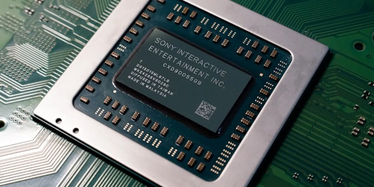
Tainan's Southern Taiwan Science Park now hosts the most advanced semiconductor fabrication complex on earth. TSMC's Fab 18, running 5nm and 3nm production at above 95% utilisation while preparing 2nm risk production, represents a concentration of manufacturing sophistication that no other geography can match. The capital commitments are staggering: NT$2.1 trillion in planned TSMC investment through 2027, with ASE and KYEC adding a combined NT$45 billion in advanced packaging expansion alongside it.
Yet the hire rate for senior technical roles in Tainan fell from 68% in 2023 to 52% in 2024. Nearly half of all critical engineering searches now end in failure. The most capital-intensive semiconductor expansion in history is running into a constraint that no amount of equipment spending can resolve: the people qualified to operate, optimise, and lead these fabrication lines do not exist in sufficient numbers, and the ones who do exist are almost entirely unreachable through conventional hiring.
What follows is a ground-level analysis of the forces reshaping Tainan's semiconductor talent market in 2026, the specific roles and skills where the gap is most severe, and what organisations operating in or hiring for this cluster need to understand before they commit to their next search. The picture that emerges is one where capital has moved faster than human capital could follow, and the consequences are now visible in every hiring metric that matters.
The Capital That Built the World's Most Advanced Fabs Cannot Build the Workforce to Run Them
The scale of investment flowing into Tainan's semiconductor cluster is difficult to overstate. TSMC's Fab 18 alone, at full build-out, will process over 200,000 twelve-inch wafers per month. Fab 14 adds another 40,000. Together they employ approximately 28,000 people within a science park whose total headcount reached 38,000 by Q3 2024. TSMC is not merely the anchor tenant of the Southern Taiwan Science Park. It is the gravitational centre around which an entire ecosystem of equipment maintenance firms, specialty chemical suppliers, and mask shops has formed.
The 2026 outlook intensifies this concentration. TSMC's 2nm node, designated N2, began risk production in late 2025 and is entering volume ramp this year at Fab 18 Phase 6. That ramp requires an additional 3,500 to 4,000 process engineers and equipment technicians in Tainan alone. Simultaneously, ASE Technology Holding's new advanced packaging facility in the Luzhu district, focused on 3DIC and hybrid bonding architectures, plans to bring on 800 to 1,000 engineers by mid-2026.
Against this demand, the supply picture is stark. The talent gap ratio in 2024 stood at 1.52 to 1: 18,400 open semiconductor positions against 12,100 candidates with relevant experience, according to 104 Job Bank's 2024 Semiconductor Industry Talent Report. And that ratio describes the aggregate market, including operational roles where supply is adequate. At the senior engineering and executive level, the ratio is far worse. The fill rate decline from 68% to 52% in a single year tells the real story. Capital deployment is accelerating. Talent absorption is decelerating. The gap between them is widening precisely at the moment when the most advanced production nodes demand the most specialised people.
This is the core analytical tension of Tainan's semiconductor market in 2026: the investment in 2nm and advanced packaging has not reduced the need for experienced engineers. It has replaced one category of engineer with another that does not yet exist in sufficient numbers. Every dollar of capital committed to next-generation fabrication creates demand for skills that were not taught five years ago, cannot be acquired without access to specific toolsets, and are held by a population so small that 95% of the most critical specialists are not looking for a new role.
Where the Shortage Is Most Acute: Three Roles That Define the Bottleneck
EUV Lithography Engineers
The single hardest role to fill in Tainan's semiconductor market is the senior EUV lithography engineer. These are specialists with five to ten years of experience operating and optimising ASML's NXE:3600D and NXE:3800E scanners, managing light source stability, and troubleshooting the extreme ultraviolet exposure process that makes sub-5nm fabrication possible. Their unemployment rate is below 0.5%. Their average tenure at current employers is 7.2 years. An estimated 95% are passive candidates who will never respond to a job posting.
Compensation reflects the scarcity. EUV specialists at the senior manager level command NT$2.5 million to NT$4.0 million in total annual compensation, a 30% to 40% premium over standard process engineering roles at equivalent seniority. At the executive level, packages reach NT$6 million to NT$10 million.
The problem is not that firms are unwilling to pay. The problem is that the global population of engineers with deep EUV process experience numbers in the low thousands, and a meaningful share of them are already in Tainan working for TSMC. Recruiting from this pool requires not a job advertisement but a direct headhunting approach with months of relationship-building before a candidate will even consider a conversation.
Process Integration Engineers for 3nm and 2nm Nodes
Process integration at the 3nm and 2nm level demands mastery of gate-all-around transistor architecture, nanosheet width control, inner spacer engineering, and Cu/low-k integration through chemical mechanical planarisation. These are not skills that can be acquired through academic training alone. They require hands-on experience with production-grade tooling at the relevant node.
The circular problem is obvious: the only place to gain 2nm experience is at a facility running 2nm production, and the only facility running 2nm production in 2026 is TSMC Fab 18 in Tainan. Every other employer competing for this talent is asking candidates to transfer skills from adjacent nodes. TSMC itself must develop much of this capability internally, which constrains the speed at which the broader ecosystem can staff up.
Advanced Packaging Integration Architects
The third critical shortage sits at the intersection of front-end fabrication and back-end packaging. As chiplet architectures and 3DIC integration become central to AI accelerator design, the engineers who understand hybrid bonding alignment precision, wafer-to-wafer bonding defect density targets, and through-silicon via architecture are in acute demand. ASE's Tainan expansion is built around these skills. KYEC's testing operations increasingly require engineers who understand what happens upstream in packaging, not just downstream in probe card optimisation.
The passive candidate ratio here is 85%. Active applicants tend to be recent graduates with fewer than three years of experience or career switchers from unrelated fields. Senior architects with hybrid bonding expertise are employed, well-compensated, and content. Moving them requires equity participation, sabbatical guarantees, or a technology roadmap they cannot access in their current role. The cost of a bad executive hire in a market this thin is not merely financial. It sets the hiring organisation back months in a race measured in quarters.
The Three-Front Talent War Draining Tainan's Pipeline
Tainan's talent crisis would be severe even if the city were competing only with itself. It is not. The market faces simultaneous competitive pressure from three distinct geographies, each pulling candidates away through a different mechanism.
[Hsinchu](/hsinchu-taiwan-executive-search)'s Gravitational Pull
Hsinchu Science Park, home to TSMC's headquarters and central R&D operations, offers 15% to 20% base salary premiums for equivalent roles at non-TSMC firms. Senior process engineers in Hsinchu average NT$2.8 million in total compensation against NT$2.4 million for comparable positions in Tainan. But the salary gap is only part of the draw. Hsinchu offers superior career trajectory visibility. Proximity to TSMC's R&D centre means proximity to promotion decisions, strategic direction-setting, and the informal networks that determine who gets tapped for leadership roles. For international talent, Hsinchu's denser international schooling and expatriate amenities remove a practical barrier that Tainan has not yet addressed.
The result is a persistent northward drift of ambitious mid-career engineers who see Tainan as a production assignment rather than a career destination. This perception may be outdated, given that Tainan now hosts TSMC's most advanced node. But perception shapes behaviour, and behaviour shapes the talent pool.
[Taichung](/taichung-taiwan-executive-search)'s Quality-of-Life Advantage
Central Taiwan Science Park in Taichung presents a different competitive proposition. TSMC's Fab 15 runs 28nm and 7nm production there, and newer expansions are adding capacity. Taichung offers newer residential infrastructure, lower cost of living than Tainan's congested southern districts, and measurably better retention: turnover rates for equivalent packaging roles run 12% lower than in Tainan, according to the National Science and Technology Council's 2024 employment stability data. For a mid-career engineer weighing two offers at similar compensation, Taichung's liveability advantage can be decisive.
The Overseas Multiplier
The most damaging competitive pressure comes from offshore. TSMC's Arizona Fab 21 and Japan's JASM facility in Kumamoto offer Mandarin-speaking Taiwanese engineers 2.5 to 3.0 times their Tainan total compensation, with additional housing and education subsidies. According to Nikkei Asia's January 2025 reporting, an estimated 1,800 to 2,200 senior engineers from the Tainan talent pool had accepted overseas assignments by Q4 2024.
This is not a temporary spike. It is a systemic drain. And the retention lever that Tainan employers use to counter it reveals the market's deepest structural feature: they compete not on cash, which is unwinnable against US multiples, but on technology access. Engineers who stay in Tainan gain 2nm and 1.4nm node experience that will not be available in overseas fabs until 2027 or 2028. Profit-sharing vesting schedules that penalise early departure add a financial lock-in. But for every engineer who stays for the technology, another leaves for the money. The net effect is a talent pool that shrinks even as the capital base expands.
Compensation Bifurcation: The TSMC Premium and What It Means for Everyone Else
The compensation data in Tainan's semiconductor market tells two very different stories depending on whether the employer is TSMC.
TSMC's 2024 employee profit sharing averaged NT$5.01 million per employee across all levels. Combined with base salary and bonuses, this creates a total compensation gap of approximately 40% to 60% above equivalent roles at KYEC or ASE for mid-level engineers, and 80% to 100% at executive levels. A senior specialist at TSMC in front-end process engineering earns NT$2.2 million to NT$3.5 million in total compensation. The same role at a non-TSMC fabrication firm pays NT$1.6 million to NT$2.4 million. At the VP level, the gap widens further: NT$8 million to NT$15 million at TSMC against NT$4.5 million to NT$7 million elsewhere.
For packaging and testing firms, the numbers are lower still. Senior specialists at ASE or KYEC earn NT$1.5 million to NT$2.3 million. Executives reach NT$3.8 million to NT$6.5 million. These are respectable packages by Taiwanese standards. They are not competitive with TSMC.
The implication for hiring is severe. Non-TSMC employers in Tainan are not competing on a level field. They cannot match TSMC's profit-sharing model, which is a function of TSMC's extraordinary margins on leading-edge production. What they can offer is different work: advanced packaging R&D that TSMC outsources, testing expertise that TSMC does not develop in-house, and leadership roles with broader operational scope than a process engineer might find inside TSMC's more hierarchical structure. But communicating that value proposition to a passive candidate requires reaching them first, which brings the conversation back to how searches are conducted.
The research is unambiguous on this point. At the Fab Operations VP level, the market is described as 100% passive or closed. No active job posting yields a qualified applicant. All placements originate from board-level executive search mandates targeting specific individuals. The question is not whether to use executive search. The question is whether the search method is fast enough and precise enough to reach the right person before a competitor does.
For organisations navigating these compensation benchmarks across the semiconductor sector, understanding the TSMC premium is not optional. It defines the floor of every negotiation.
Infrastructure Fragility: The Paradox Underneath the Production Lines
Tainan hosts the world's most advanced, margin-sensitive semiconductor production. It simultaneously exhibits Taiwan's most fragile power and water infrastructure. This is not a minor irony. It is a strategic contradiction that affects every hiring conversation at the executive level.
The Bureau of Energy flagged Southern Taiwan's grid reserve margins at 6.8% in summer 2024, well below the 10% safety threshold. A turbine failure at the Hsinta Power Plant caused 2.4-hour outages at three non-TSMC suppliers, resulting in NT$120 million in yield losses. The Datang ultra-high-voltage substation, projected for completion in Q4 2026, is the infrastructure answer. Until it arrives, fabs face forced curtailment risks during peak demand periods.
Water constraints are equally acute. The 2023-2024 drought forced TSMC to deploy tanker trucks at a cost of NT$200 million monthly. Reservoir levels have recovered, but the Water Resources Agency maintains Stage 1 conservation alerts for Tainan, mandating fab recycling rates above 90%. Those recycling mandates add NT$0.8 to NT$1.2 per wafer in treatment costs.
Land scarcity compounds both problems. STSP Phase 1 and Phase 2 stand at 98.7% occupancy. TSMC's upcoming 2nm expansion at Fab 18 Phases 5-6 will use the final available plots. Subsequent growth depends on the Phase 3 land reclamation project, which faces legal challenges from local farmers and environmental groups. Judicial injunctions delayed ground-breaking by eight months in 2024.
Why does infrastructure matter in an article about talent? Because the executives qualified to run these operations understand these risks intimately. A VP of Fab Operations in Tainan is not merely managing 20,000 employees and $50 billion in capital. They are managing operational continuity in a geography where a single drought season or a single grid failure can erase hundreds of millions in output. The calibre of leader required for this environment is not the same as what a stable-infrastructure fab in Arizona or Kumamoto demands. The talent mapping required to identify them must account for this operational complexity, not just technical credentials.
What This Means for Organisations Hiring in Tainan's Semiconductor Market
The conventional approach to filling semiconductor engineering and leadership roles follows a predictable pattern: post a vacancy on 104 Job Bank or 1111 Job Bank, wait for applications, screen, interview, offer. In Tainan's current market, this approach reaches at most the 5% to 15% of qualified candidates who happen to be actively looking. The other 85% to 95%, the ones with the experience, the node exposure, and the track record that actually matter, are invisible to it.
The pattern of "phantom job postings" documented in 104 Job Bank's 2024 passive recruitment analysis illustrates the dysfunction. TSMC and major OSATs maintain permanent vacancy listings for EUV senior engineers without immediate intention to fill, using them as candidate funnels for pipeline development six to twelve months out. This means the job board ecosystem is polluted with postings that are not real vacancies, making it harder for genuine hiring efforts to stand out.
According to Commercial Times reporting in November 2024, KYEC maintained an open requisition for a Senior Advanced Testing Engineer for 217 days, more than double the 89-day industry average, despite offering relocation packages and NT$300,000 signing bonuses. The role remained unfilled. The problem was not compensation. It was access. The candidates who could fill it were employed, passive, and unreachable through any channel KYEC was using.
Meanwhile, Liberty Times reported in October 2024 that ASE recruited a Process Integration Manager from a competitor's Tainan facility by offering a 65% compensation premium: a total package of NT$4.8 million against a market rate of NT$2.9 million. That single hire reportedly triggered the departure of four additional senior engineers from the target firm within six months. In a market this thin, one aggressive hire creates cascading retention crises.
For organisations that need to fill senior semiconductor leadership roles in this environment, the lesson is clear. Speed matters. Method matters more. The firms that reach the right candidate first, with a proposition calibrated to what that specific individual values, will fill the role. The firms that wait for applications will not.
The risk of a prolonged vacancy in Tainan is not abstract. It is measured in wafer output delayed, packaging lines understaffed, and capital equipment sitting idle because the engineers who operate it have not been found.
How KiTalent Approaches Executive Search in Semiconductor Markets
KiTalent's AI-enhanced direct headhunting methodology is designed for exactly the market conditions Tainan presents: extreme passive candidate dominance, compressed hiring windows, and a talent pool where 95% of the most qualified individuals will never see a job posting. By combining AI-powered talent mapping with direct outreach to identified individuals, KiTalent delivers interview-ready executive candidates within 7 to 10 days. Clients pay per interview, not through upfront retainers, which removes the financial risk of a search that does not produce the right candidates.
In markets where a single senior hire can trigger a cascade of competitive departures, the 96% one-year retention rate that KiTalent maintains across its 1,450+ completed executive placements matters as much as speed. A hire that stays is worth more than a hire that arrives quickly and leaves within the year.
For organisations competing for EUV lithography specialists, advanced packaging architects, or fab operations leadership in Tainan's semiconductor cluster, where the candidates who matter most are not visible on any job board and the cost of a slow search is measured in production delays and cascading retention losses, speak with our semiconductor executive search team about how we approach this market.
Frequently Asked Questions
What is the current talent gap ratio in Tainan's semiconductor sector?
As of 2024, Tainan recorded 18,400 open semiconductor positions against 12,100 available candidates with relevant experience, a gap ratio of 1.52 to 1 according to 104 Job Bank. This aggregate figure understates the severity at senior levels. For EUV lithography engineers with five or more years of experience, the passive candidate rate reaches 95%, meaning almost none are reachable through conventional job postings. The fill rate for senior technical roles dropped from 68% in 2023 to 52% in 2024, indicating that the gap is widening as advanced node expansion accelerates demand for specialists who do not yet exist in sufficient numbers.
What do senior semiconductor engineers earn in Tainan?
Total annual compensation varies substantially by employer. At TSMC, senior specialists in front-end process engineering earn NT$2.2 million to NT$3.5 million, while VP-level roles reach NT$8 million to NT$15 million. Non-TSMC fabrication firms pay NT$1.6 million to NT$2.4 million at the senior specialist level and NT$4.5 million to NT$7 million for executives. EUV lithography specialists command a 30% to 40% premium over standard process roles. TSMC's profit-sharing model, which averaged NT$5.01 million per employee in 2024, creates a compensation gap of 40% to 100% above equivalent roles at packaging and testing firms.
Why is it so difficult to hire EUV lithography engineers in Southern Taiwan?
EUV lithography engineers represent one of the smallest, most specialised talent pools in the global semiconductor industry. Their unemployment rate is below 0.5% and their average tenure at current employers is 7.2 years. Approximately 95% are passive candidates who do not respond to vacancy postings. Recruitment in this segment occurs exclusively through direct headhunting and executive search with three-to-six-month lead times. The global population of engineers with deep EUV process experience numbers in the low thousands, and many are already employed by TSMC in Tainan.
How does Tainan compete with overseas fabs for semiconductor talent?
Tainan cannot compete on cash compensation. TSMC's Arizona and Japan facilities offer 2.5 to 3.0 times Tainan total compensation for senior engineers willing to relocate. Instead, Tainan employers compete on technology access. Engineers who remain in Tainan gain hands-on experience with 2nm and future 1.4nm nodes that will not be available in overseas fabs until 2027 or 2028. Profit-sharing vesting schedules that penalise early departure add financial lock-in. Despite these levers, an estimated 1,800 to 2,200 senior engineers left the Tainan talent pool for overseas assignments by late 2024.
How can KiTalent help with semiconductor executive hiring in Tainan?
KiTalent uses AI-enhanced direct headhunting to identify and reach passive candidates who represent 85% to 95% of the qualified talent pool in Tainan's semiconductor sector. The methodology delivers interview-ready candidates within 7 to 10 days, with a pay-per-interview model that removes upfront retainer risk. With a 96% one-year retention rate across 1,450+ placements, KiTalent addresses both the speed and durability requirements of semiconductor executive search. For firms seeking EUV specialists, advanced packaging leaders, or fab operations executives in Southern Taiwan, connecting with our team is the first step toward reaching candidates that conventional channels cannot.
What infrastructure risks affect semiconductor operations and hiring in Tainan?
Tainan faces three converging infrastructure constraints. Power grid reserve margins fell to 6.8% in Southern Taiwan in 2024, below the 10% safety threshold, with a critical substation upgrade not expected until late 2026. Water supply remains under Stage 1 conservation alerts, requiring fab recycling rates above 90%. Land at STSP is 98.7% occupied, with expansion dependent on a legally contested land reclamation project. These risks directly affect executive hiring because the calibre of leader required to manage operations under these conditions is materially higher than what a stable-infrastructure facility demands.